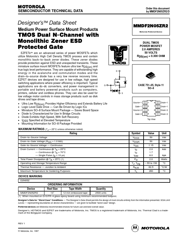
lieved readily achievable with board mounted components. Most power electronic loads are inductive; the data in the figure is taken with a resistive load, which approximates an optimally snubbed inductive load. Power MOSFETs may be safely operated into an inductive load; however, snubbing reduces switching losses. 250
VDS = 0 V Ciss
VGS = 0 V
TJ = 25°C
200 C,.
The following content is an automatically extracted verbatim text
from the original manufacturer datasheet and is provided for reference purposes only.
View original datasheet text
MOTOROLA
SEMICONDUCTOR TECHNICAL DATA
Order this document by MMDF2N05ZR2/D
Designer's
™ Data Sheet
Medium Power Surface Mount Products
MMDF2N05ZR2
Motorola Preferred Device
TMOS Dual N-Channel with Monolithic Zener ESD Protected Gate
EZFETs™ are an advanced series of power MOSFETs which utilize Motorola’s High Cell Density TMOS process and contain monolithic back–to–back zener diodes. These zener diodes provide protection against ESD and unexpected transients. These miniature surface mount MOSFETs feature ultra low RDS(on) and true logic level performance. They are capable of withstanding high energy in the avalanche and commutation modes and the drain–to–source diode has a very low reverse recovery time.