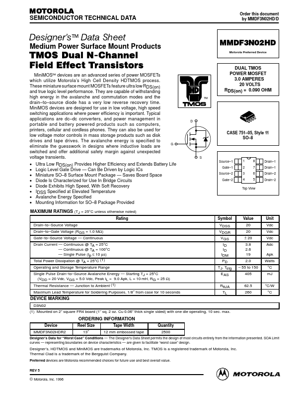
fied. The resistive switching time variation versus gate resistance (Figure 9) shows how typical switching performance is affected by the parasitic circuit elements. If the parasitics were not present, the slope of the curves would maintain a value of unity regardless of the switching speed. The circuit used to obtain the data is constructed to minimize common inductance in the drain and gate circuit loops and is believed readily achievable with board mounted components. Most power electronic lo.
Full PDF Text Transcription for MMDF3N02HD (Reference)
Note: Below is a high-fidelity text extraction (approx. 800 characters) for
MMDF3N02HD. For precise diagrams, and layout, please refer to the original PDF.
MOTOROLA SEMICONDUCTOR TECHNICAL DATA Order this document by MMDF3N02HD/D Designer's ™ Data Sheet Medium Power Surface Mount Products MMDF3N02HD Motorola Preferred Device...
View more extracted text
dium Power Surface Mount Products MMDF3N02HD Motorola Preferred Device TMOS Dual N-Channel Field Effect Transistors MiniMOS™ devices are an advanced series of power MOSFETs which utilize Motorola’s High Cell Density HDTMOS process. These miniature surface mount MOSFETs feature ultra low RDS(on) and true logic level performance. They are capable of withstanding high energy in the avalanche and commutation modes and the drain–to–source diode has a very low reverse recovery time. MiniMOS devices are designed for use in low voltage, high speed switching applications where power efficiency is important.