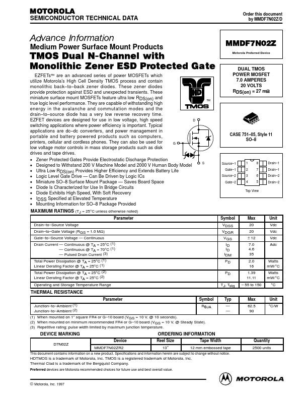
fied. The resistive switching time variation versus gate resistance (Figure 9) shows how typical switching performance is affected by the parasitic circuit elements. If the parasitics were not present, the slope of the curves would maintain a value of unity regardless of the switching speed. The circuit used to obtain the data is constructed to minimize common inductance in the drain and gate circuit loops and is believed readily achievable with board mounted components. Most power electronic lo.
The following content is an automatically extracted verbatim text
from the original manufacturer datasheet and is provided for reference purposes only.
View original datasheet text
MOTOROLA
SEMICONDUCTOR TECHNICAL DATA
Order this document by MMDF7N02Z/D
Advance Information
Medium Power Surface Mount Products
MMDF7N02Z
Motorola Preferred Device
TMOS Dual N-Channel with Monolithic Zener ESD Protected Gate
EZFETs™ are an advanced series of power MOSFETs which utilize Motorola’s High Cell Density TMOS process and contain monolithic back–to–back zener diodes. These zener diodes provide protection against ESD and unexpected transients. These miniature surface mount MOSFETs feature ultra low RDS(on) and true logic level performance. They are capable of withstanding high energy in the avalanche and commutation modes and the drain–to–source diode has a very low reverse recovery time.