Motorola MMSF10N02Z
SINGLE TMOS POWER MOSFET
| Part No. | MMSF10N02Z |
|---|---|
| Datasheet | MMSF10N02Z Download |
| Manufacturer |  Motorola |
| Description | SINGLE TMOS POWER MOSFET |
| Buy | Stock & Price |
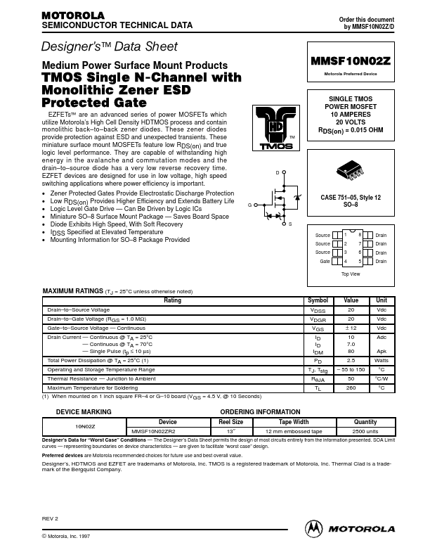
MAXIMUM RATINGS
(TJ = 25°C unless otherwise noted) Rating Drain–to–Source Voltage Drain–to–Gate Voltage (RGS = 1.0 MΩ) Gate–to–Source Voltage — Continuous Drain Current — Continuous @ TA = 25°C Drain Current — Continuous @ TA = 70°C Drain Current — Single Pulse (tp ≤ 10 µs) Total Power Dissipation @ TA = 25°C (1) Operating and Storage Temperature Range Thermal Resistance — Junction to Ambient Maximum Temperature for Soldering (1) When mounted on 1 inch square FR–4 or G–10 board (VGS = 4.5 V, @ 10 Seconds) Symbol VDSS VDGR VGS ID ID IDM PD TJ, Tstg RθJA TL Value 20 20 ± 12 10 7.0 80 2.5 – 55 to 150 50 260 Unit Vdc Vdc Vdc Adc Apk Watts °C °C/W °C DEVICE MARKING 10N02Z Device MMSF10N02ZR2 ORDERING INFORMATION Reel Size 13″ Tape Width 12 mm embossed tape Quantity 2500 units Designer’s Data for “Worst Case” Conditions — The Designer’s Data Sheet permits the design of most circuits entirely from the information presented. SOA Limit curves — representing boundaries on device characteristics — are given to facilitate “worst case” design.