onsemi MMSF10N02Z
Power MOSFET
| Part No. | MMSF10N02Z |
|---|---|
| Datasheet | MMSF10N02Z Download |
| Manufacturer |  onsemi |
| Description | Power MOSFET |
| Buy | Stock & Price |
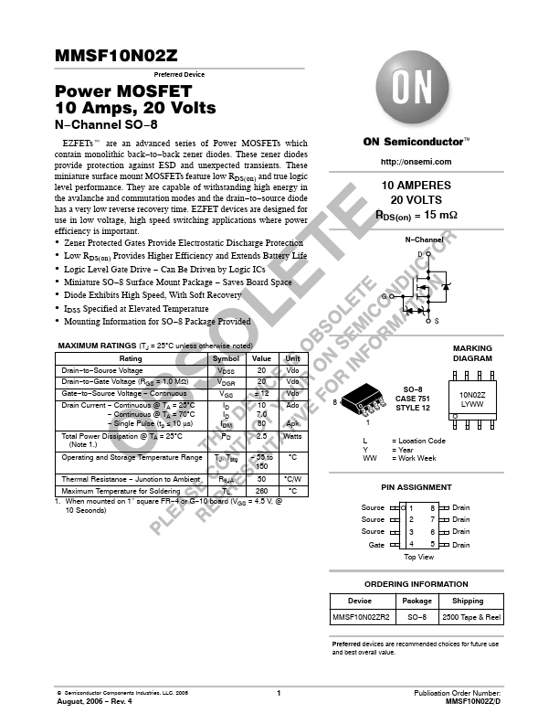
MAXIMUM RATINGS
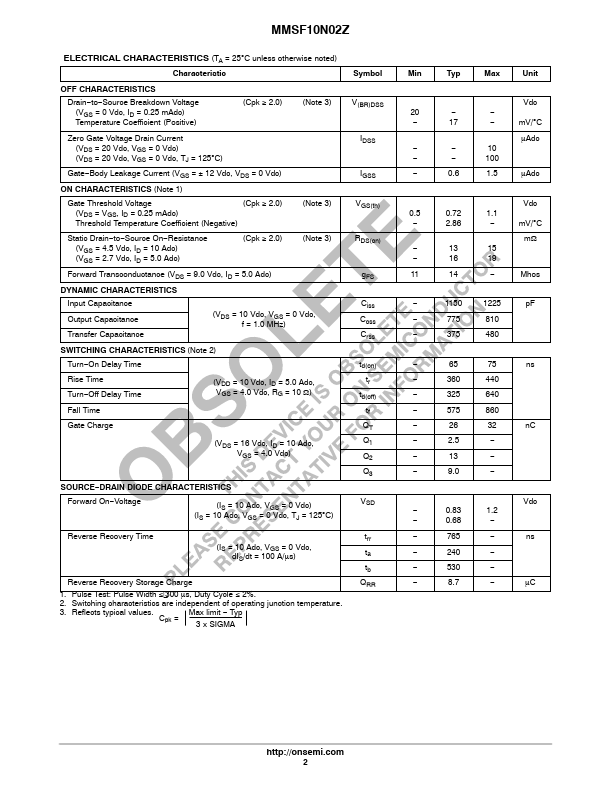
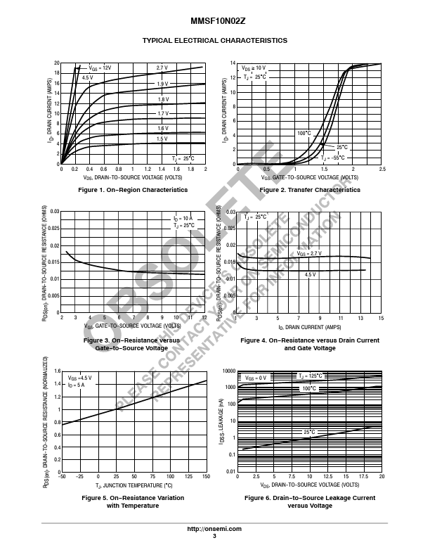
(TJ = 25°C unless otherwise noted) Rating Symbol Value Unit Drain−to−Source Voltage Drain−to−Gate Voltage (RGS = 1.0 MΩ) Gate−to−Source Voltage − Continuous Drain Current − Continuous @ TA = 25°C Drain Current − Continuous @ TA = 70°C Drain Current − Single Pulse (tp ≤ 10 μs) Total Power Dissipation @ TA = 25°C (Note 1.) VDSS VDGR VGS ID ID IDM PD 20 Vdc 20 Vdc ± 12 Vdc 10 Adc 7.0 80 Apk 2.5 Watts Operating and Storage Temperature Range TJ, Tstg − 55 to 150 °C Thermal Resistance − Junction to Ambient RθJA 50 °C/W Maximum Temperature for Soldering TL 260 °C 1. When mounted on 1″ square FR−4 or G−10 board (VGS = 4.5 V, @ 10 Seconds) 10 AMPERES 20 VOLTS RDS(on) = 15 mW N−Channel D G S MARKING DIAGRAM 8 SO−8 CASE 751 STYLE 12 10N02Z LYWW 1 L = Location Code Y = Year WW = Work Week PIN ASSIGNMENT Source Source Source Gate 18 27 36 45 Top View Drain Drain Drain Drain ORDERING INFORMATION Device Package Shipping MMSF10N02ZR2 SO−8 2500 Tape & Reel Preferred devices are recommended choices for future use and best overall value. © Semiconductor Components Industries, LLC, 2006 August, 2006 − Rev.