MPC2106B
Key Features
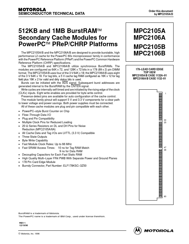
- PowerPC–style Burst Counter on Chip Flow–Through Data I/O Plug and Pin patibility Multiple Clock Pins for Reduced Loading 20 Ω Series Resistors on DL and DH Pins for Noise Reduction (MPC2105A/6A) All Cache Data and Tag I/Os are LVTTL (3.3 V) patible Three State Outputs Byte Write Capability Fast Module Clock Rates: Up to 66 MHz Fast SRAM Access Times: 10 ns for Tag RAM Match 9 ns for Data RAM Decoupling Capacitors for Each Fast Static RAM High Quality Multi–Layer FR4 PWB With Separate Power and Ground Planes 178 Pin Card Edge Module Burndy Connector, Part Number: ELF178KSC–3Z50