MPC9120
MPC9120 is 1:10 LVCMOS FANOUT BUFFER manufactured by Motorola Semiconductor.
features
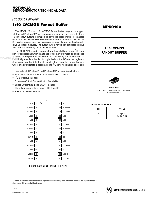
10 low skew outputs optimized to drive the clock inputs of standard unbuffered SO- DIMM SDRAM modules. Standard unbuffered SO- DIMM SDRAM modules require two clocks per module allowing for the device to drive up to four modules. The output buffers have been optimized to drive the load presented by the SDRAM module. The MPC9120 provides output shut off capabilities via an I2C serial port for applications which plan to use fewer than four modules and desire to minimize the power dissipation of the chip. Every output clock can be .. individually enabled/disabled through fields in the I2C control registers. After power up the default state is all outputs enabled. In applications where this default state is acceptable the I2C ports need not be exercised.
1:10 LVCMOS FANOUT BUFFER
- -
- -
- -
- Supports Intel Pentium™ and Pentium II Processor Architectures 10 Skew Controlled 3.3V patible SDRAM Clocks I2C Serial Bus Interface Extensive Output Enable Control Capability Space Efficient 28- Lead SSOP Package Operating Temperature Range of 0°C to 70°C 3.3V ± 5% Power Supply
SD SUFFIX 28- LEAD PLASTIC SSOP PACKAGE CASE 940E- 02
VDD SDRAM0 SDRAM1 VSSO VDD SDRAM2 SDRAM3 VSS BUF_IN
1 2 3 4 5 6 7 8 9
28 VDD 27 SDRAM9 26 SDRAM8 25 VSS 24 VDD 23 SDRAM7 22 SDRAM6 21 VSS 20 OE 19 VDD 18 SDRAM5 17 VSS 16 VSSIIC 15 SCLOCK
FUNCTION TABLE
OE 0 1 V1, V2 High- Z 1x BUF_IN
VDD 10 SDRAM4 11 VSS 12 VDDIIC 13 SDATA 14
Figure 1. 28- Lead Pinout (Top View)
This document contains information on a product under development. Motorola reserves the right to change or discontinue this product without notice. 12/97
© Motorola, Inc. 1997
REV 0.2
SDRAM0 SDRAM1 SDRAM2 SDRAM3 SDRAM4 BUF_IN SDRAM5 SDRAM6 SDRAM7 .. SDRAM8 SDRAM9
SDATA SCLOCK
I2C INTERFACE
CONFIG REGISTERS
Figure 2. Block Diagram
Table 1. Pin Descriptions
Pin Name BUF_IN SDRAM0:9 SDATA SCLK OE VDD VSS I/O I O I/O I I
- - 3.3V CMOS clock input 3.3V CMOS SDRAM clock outputs Serial data for...