Motorola MPC9449
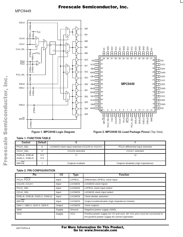
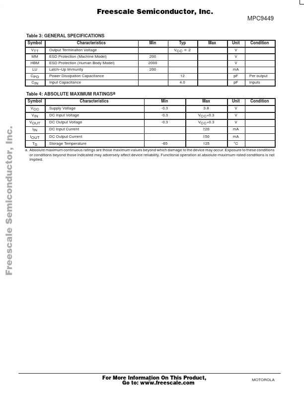
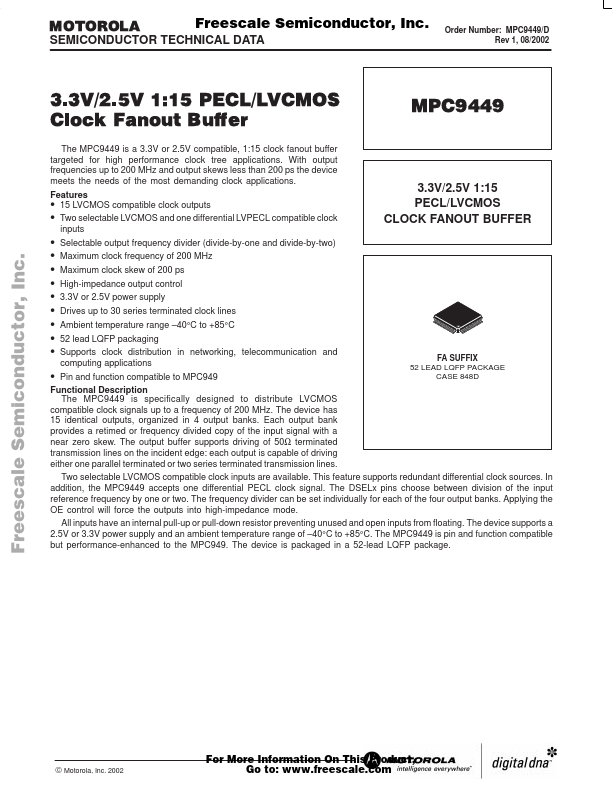
The MPC9449 is a 3.3V or 2.5V compatible, 1:15 clock fanout buffer targeted for high performance clock tree applications. With output frequencies up to 200 MHz and output skews less than 200 ps the device meets the needs of the most demanding clock applications. Supports clock distribution in networking, telecommunication and FA SUFFIX computing applications 52 LEAD LQFP PACKAGE CASE 848D • Pin and function compatible to MPC949 Functional Description The MPC9449 is specifically designed to distribute LVCMOS compatible clock signals up to a frequency of 200 MHz.| Part No. | MPC9449 |
|---|---|
| Datasheet | MPC9449 Download |
| Manufacturer |  Motorola |
| Description | 3.3V / 2.5 V 1:15 PECL/LVCMOS |
| Buy | Stock & Price |
FEATURES
● 15 LVCMOS compatible clock outputs MPC9449● Two selectable LVCMOS and one differential LVPECL compatible clock 3.3V/2.5V 1:15 PECL/LVCMOS CLOCK FANOUT BUFFER Freescale Semiconductor, Inc... The device has 15 identical outputs, organized in 4 output banks. Each output bank provides a retimed or frequency divided copy of the input signal with a near zero skew. The output buffer supports driving of 50Ω terminated transmission lines on the incident edge: each output is capable of driving either one parallel terminated or two series terminated transmission lines. Two selectable LVCMOS compatible clock inputs are available. This feature supports redundant differential clock sources. In addition, the MPC9449 accepts one differential PECL clock signal. The DSELx pins choose between division of the input reference frequency by one or two. The frequency divider can be set individually for each of the four output banks. Applying the OE control will force the outputs into high-impedance mode.