MPF930
MOTOROLA
SEMICONDUCTOR TECHNICAL DATA
Order this document by MPF930/D
TMOS Switching
N- Channel
- Enhancement
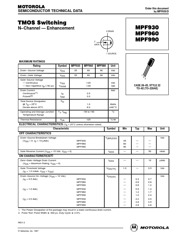
2 GATE
3 DRAIN
MPF930 MPF960 MPF990
1 SOURCE
MAXIMUM RATINGS
Rating Drain
- Source Voltage Drain
- Gate Voltage Gate- Source Voltage
- Continuous
- Non- repetitive (tp ≤ 50 µs) Drain Current Continuous(1) Pulsed(2) Total Device Dissipation @ TA = 25°C Derate above 25°C Operating and Storage Junction Temperature Range Thermal Resistance Symbol VDS VDG VGS VGSM ID IDM PD 1.0 8.0 TJ, Tstg θJA
- 55 to 150 125 Watts m W/°C °C °C/W MPF930 35 35 MPF960 60 60 ± 20 ± 40 2.0 3.0 MPF990 90 90 Unit Vdc Vdc Vdc Vpk Adc
1 2 3
CASE 29- 05, STYLE 22 TO- 92 (TO- 226AE)
ELECTRICAL CHARACTERISTICS (TA = 25°C unless otherwise noted)
Characteristic Symbol Min Typ Max Unit
OFF CHARACTERISTICS
Drain- Source Breakdown Voltage (VGS = 0, ID = 10 µAdc) V(BR)DSX MPF930 MPF960 MPF990 IGSS 35 60 90
- -
- -
- -
- - 50 n Adc Vdc
Gate Reverse Current (VGS = 15 Vdc, VDS = 0)
ON CHARACTERISTICS(2)
Zero- Gate-...