MPSA13
Overview
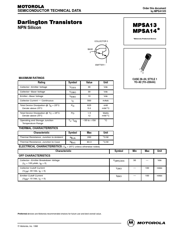
MOTOROLA SEMICONDUCTOR TECHNICAL DATA Order this document by MPSA13/D Darlington Transistors NPN Silicon COLLECTOR 3 MPSA13 MPSA14 * *Motorola Preferred Device BASE 2 EMITTER 1 1 2 3 MAXIMUM RA...
| Part | MPSA13 |
|---|---|
| Description | Darlington Transistors |
| Category | Transistor |
| Manufacturer | Motorola Semiconductor |
| Size | 225.92 KB |
MOTOROLA SEMICONDUCTOR TECHNICAL DATA Order this document by MPSA13/D Darlington Transistors NPN Silicon COLLECTOR 3 MPSA13 MPSA14 * *Motorola Preferred Device BASE 2 EMITTER 1 1 2 3 MAXIMUM RA...
| Part Number | Manufacturer | Description |
|---|---|---|
| MPSA13 | onsemi | NPN Silicon Transistor |
| MPSA13 | Central Semiconductor | SILICON NPN DARLINGTON TRANSISTORS |
| MPSA13 | Taitron Components | Small Signal Darlington Transistors |
| MPSA13 | Continental Device India | NPN EPITAXIAL PLANAR DARLINGTON TRANSISTORS |
| MPSA13 | KEC | EPITAXIAL PLANAR NPN TRANSISTOR |