MRF1535NT1
MRF1535NT1 is RF Power Field Effect Transistors manufactured by Motorola Semiconductor.
- Part of the MRF1535FNT1 comparator family.
- Part of the MRF1535FNT1 comparator family.
( Data Sheet : .. )
Freescale Semiconductor Technical Data
MRF1535T1 Rev. 7, 3/2005
RF Power Field Effect Transistors
N- Channel Enhancement- Mode Lateral MOSFETs
Designed for broadband mercial and industrial applications with frequencies to 520 MHz. The high gain and broadband performance of these devices make them ideal for large- signal, mon source amplifier applications in 12.5 volt mobile FM equipment.
- Specified Performance @ 520 MHz, 12.5 Volts Output Power
- 35 Watts Power Gain
- 10.0 d B Efficiency
- 50%
- Capable of Handling 20:1 VSWR, @ 15.6 Vdc, 520 MHz, 2 d B Overdrive
- Excellent Thermal Stability
- Characterized with Series Equivalent Large- Signal Impedance Parameters
- Broadband- Full Power Across the Band: 135- 175 MHz 400- 470 MHz 450- 520 MHz
- Broadband UHF/VHF Demonstration Amplifier Information Available Upon Request
- N Suffix Indicates Lead- Free Terminations
- 200_C Capable Plastic Package
- In Tape and Reel. T1 Suffix = 500 Units per 44 mm, 13 inch Reel.
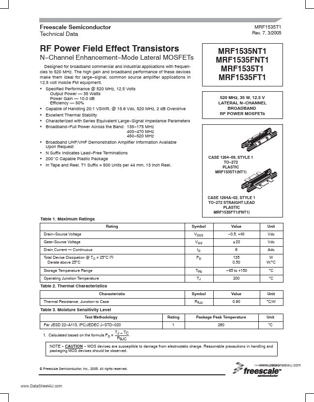
MRF1535NT1 MRF1535FNT1 MRF1535T1 MRF1535FT1
520 MHz, 35 W, 12.5 V LATERAL N- CHANNEL BROADBAND RF POWER MOSFETs
CASE 1264- 09, STYLE 1 TO- 272 PLASTIC MRF1535T1(NT1)
CASE 1264A- 02, STYLE 1 TO- 272 STRAIGHT LEAD PLASTIC MRF1535FT1(FNT1)
Table 1. Maximum Ratings
Rating Drain- Source Voltage Gate- Source Voltage Drain Current
- Continuous Total Device Dissipation @ TC = 25°C Derate above 25°C Storage Temperature Range Operating Junction Temperature
(1)
Symbol VDSS VGS ID PD Tstg TJ
Value
- 0.5, +40 ± 20 6 135 0.50
- 65 to +150 200
Unit Vdc Vdc Adc W W/°C °C °C
Table 2. Thermal Characteristics
Characteristic Thermal Resistance, Junction to Case Symbol RθJC Value 0.90 Unit °C/W
Table 3. Moisture Sensitivity Level
Test Methodology Per JESD 22- A113, IPC/JEDEC J- STD- 020 TJ
- TC 1. Calculated based on the formula PD = RθJC NOTE
- CAUTION
- MOS devices are susceptible to damage from electrostatic charge. Reasonable precautions in handling and packaging MOS devices should be observed. Rating 1 Package...