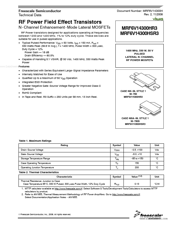
MRF6V14300HR3
MRF6V14300HR3 is RF Power Field Effect Transistors manufactured by Motorola Semiconductor.
Features
MRF6V14300HR3 MRF6V14300HSR3
1400 MHz, 330 W, 50 V PULSED LATERAL N
- CHANNEL RF POWER MOSFETs
Characterized with Series Equivalent Large
- Signal Impedance Parameters Internally Matched for Ease of Use Qualified Up to a Maximum of 50 VDD Operation Integrated ESD Protection Greater Negative Gate
- Source Voltage Range for Improved Class C Operation
- Ro HS pliant
- In Tape and Reel. R3 Suffix = 250 Units per 56 mm, 13 inch Reel.
- -
- -
- CASE 465
- 06, STYLE 1 NI
- 780 MRF6V14300HR3
CASE 465A
- 06, STYLE 1 NI
- 780S MRF6V14300HSR3
Table 1. Maximum Ratings
Rating Drain- Source Voltage Gate- Source Voltage Storage Temperature Range Case Operating Temperature Operating Junction Temperature Symbol VDSS VGS Tstg TC TJ Value
- 0.5, +100
- 6.0, +10
- 65 to +150 150 200 Unit Vdc Vdc °C °C °C
Table 2. Thermal Characteristics
Characteristic Thermal Resistance, Junction to Case Case Temperature 65°C, 330 W Pulsed, 300 μsec Pulse Width, 12% Duty Cycle Symbol RθJC Value (1,2) 0.13 Unit °C/W
1. MTTF calculator available at http://.freescale./rf. Select Software & Tools/Development Tools/Calculators to access MTTF calculators by product. 2. Refer to AN1955, Thermal Measurement Methodology of RF Power Amplifiers. Go to http://.freescale./rf. Select Documentation/Application Notes
- AN1955.
© Freescale Semiconductor, Inc., 2008. All rights reserved.
MRF6V14300HR3 MRF6V14300HSR3 1
RF Device Data Freescale Semiconductor
Table 3. ESD Protection Characteristics
Test Methodology Human Body Model (per JESD22
- A114) Machine Model (per EIA/JESD22
- A115) Charge Device Model (per JESD22
- C101) Class 1C (Minimum) A (Minimum) IV (Minimum)
Table 4. Electrical Characteristics (TC = 25°C unless otherwise noted)
Characteristic Off Characteristics Gate- Source Leakage Current (VGS = 5 Vdc, VDS = 0 Vdc) Drain- Source Breakdown Voltage (VGS = 0 Vdc, ID = 100 m A) Zero Gate Voltage Drain Leakage Current .. (VDS = 50 Vdc, VGS = 0 Vdc) Zero Gate Voltage Drain Leakage Current (VDS...