Datasheet4U Logo Datasheet4U.com

MTD20N06HDL - Power MOSFET

Key Features

  • speed. The circuit used to obtain the data is constructed to minimize common inductance in the drain and gate circuit loops and is believed readily achievable with board mounted components. Most power electronic loads are inductive; the data in the figure is taken with a resistive load, which approximates an optimally snubbed inductive load. Power MOSFETs may be safely operated into an inductive load; however, snubbing reduces switching losses. VDS = 0 V VGS = 0 V TJ = 25°C GATE.
  • TO.

📥 Download Datasheet

Full PDF Text Transcription (Reference)

The following content is an automatically extracted verbatim text from the original manufacturer datasheet and is provided for reference purposes only.

View original datasheet text
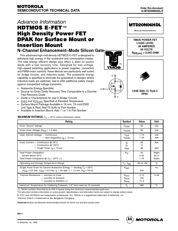
MOTOROLA SEMICONDUCTOR TECHNICAL DATA Order this document bt MTD20N06HDL/D Advance Information HDTMOS E-FETāā™ High Density Power FET DPAK for Surface Mount or Insertion Mount N–Channel Enhancement–Mode Silicon Gate This advanced high–cell density HDTMOS E–FET is designed to withstand high energy in the avalanche and commutation modes. The new energy efficient design also offers a drain–to–source diode with a fast recovery time. Designed for low–voltage, high–speed switching applications in power supplies, converters and PWM motor controls, these devices are particularly well suited for bridge circuits, and inductive loads.