MTP15N06V
MTP15N06V is TMOS POWER FET manufactured by Motorola Semiconductor.
Features of TMOS V
- On- resistance Area Product about One- half that of Standard MOSFETs with New Low Voltage, Low RDS(on) Technology
- Faster Switching than E- FET Predecessors Features mon to TMOS V and TMOS E- FETS
- Avalanche Energy Specified
- IDSS and VDS(on) Specified at Elevated Temperature
- Static Parameters are the Same for both TMOS V and TMOS E- FET MAXIMUM RATINGS (TC = 25°C unless otherwise noted)
Rating Drain- Source Voltage Drain- Gate Voltage (RGS = 1.0 MΩ) Gate- Source Voltage
- Continuous Gate- Source Voltage
- Single Pulse (tp ≤ 50 µs) Drain Current
- Continuous @ 25°C Drain Current
- Continuous @ 100°C Drain Current
- Single Pulse (tp ≤ 10 µs) Total Power Dissipation @ 25°C Derate above 25°C Operating and Storage Temperature Range Single Pulse Drain- to- Source Avalanche Energy
- Starting TJ = 25°C (VDD = 25 Vdc, VGS = 10 Vdc, IL = 15 Apk, L = 1.0 m H, RG = 25 Ω) Thermal Resistance
- Junction to Case Thermal Resistance
- Junction to Ambient
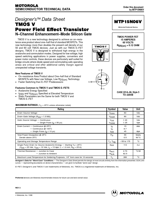
G S CASE 221A- 06, Style 5 TO- 220AB
Symbol VDSS VDGR VGS VGSM ID ID IDM PD TJ, Tstg EAS RθJC RθJA TL
Value 60 60 ± 20 ± 25 15 8.7 45 55 0.5
- 55 to 175 113 2.73 62.5 260
Unit Vdc Vdc Vdc Vpk Adc Apk Watts W/°C °C m J °C/W °C
Maximum Lead Temperature for Soldering Purposes, 1/8″ from case for 10 seconds
Designer’s Data for “Worst Case” Conditions
- The Designer’s Data Sheet permits the design of most circuits entirely from the information presented. SOA Limit curves
- representing boundaries on device characteristics
- are given to facilitate “worst case” design.
E- FET, Designer’s and TMOS V are trademarks of Motorola, Inc. TMOS is a registered trademark of Motorola, Inc.
Preferred devices are Motorola remended choices for future use and best overall value.
REV 2
TMOS © Motorola Motorola, Inc. 1996
Power MOSFET Transistor Device Data
ELECTRICAL CHARACTERISTICS (TJ = 25°C unless otherwise noted)
Characteristic OFF CHARACTERISTICS Drain- Source Breakdown Voltage (VGS = 0 Vdc, ID = 250 µAdc)...