SN74LS367A Overview
Key Specifications
Package: SOP
Mount Type: Surface Mount
Pins: 16
Operating Voltage: 5 V
| Part | SN74LS367A |
|---|---|
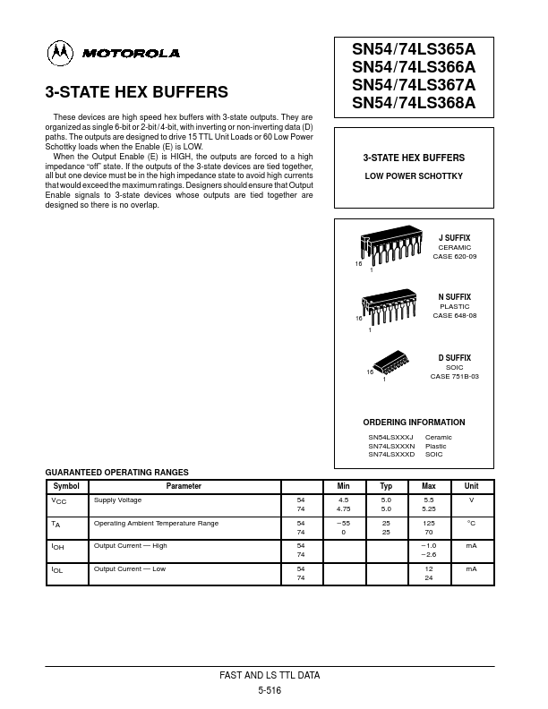
| Description | 3-STATE HEX BUFFERS |
| Manufacturer | Motorola Semiconductor |
| Size | 148.01 KB |
Package: SOP
Mount Type: Surface Mount
Pins: 16
Operating Voltage: 5 V
| Seller | Inventory | Price Breaks | Buy |
|---|---|---|---|
| Rochester Electronics | 14915 | 100+ : 1.01 USD 500+ : 0.909 USD 1000+ : 0.8383 USD 10000+ : 0.7474 USD |
View Offer |
| Verical | 1000 | 298+ : 1.2625 USD 500+ : 1.1363 USD 1000+ : 1.0479 USD 10000+ : 0.9343 USD |
View Offer |
| Part Number | Manufacturer | Description |
|---|---|---|
| SN74LS367A | onsemi | 3-State Hex Buffer |
| SN74LS367A | Texas Instruments | Hex Bus Driver |
| SN74LS365A | onsemi | 3-State Hex Buffer |
| SN74LS368A | onsemi | 3-State Hex Buffer |
| SN74LS366A | Texas Instruments | Hex Bus Driver |