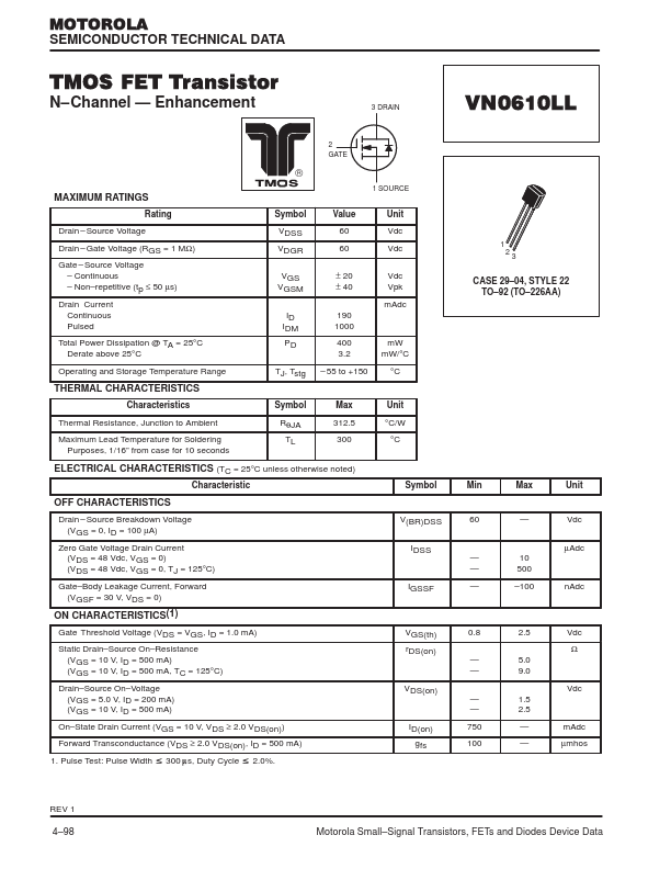
VN0610LL Overview
Key Specifications
Package: SOT-23-3
Height: 4.7 mm
Length: 4.7 mm
Width: 3.68 mm
Key Features
- Source Voltage
- Gate Voltage (RGS = 1 MΩ)
| Part | VN0610LL |
|---|---|
| Description | TMOS FET Transistor |
| Category | Transistor |
| Manufacturer | Motorola Semiconductor |
| Size | 50.22 KB |
Package: SOT-23-3
Height: 4.7 mm
Length: 4.7 mm
Width: 3.68 mm
| Seller | Inventory | Price Breaks | Buy |
|---|---|---|---|
| Component Stockers USA | 569 | 1+ : 99.99 USD | View Offer |
| Worldway Electronics | 27007 | 7+ : 0.2825 USD 10+ : 0.2768 USD 100+ : 0.2684 USD 500+ : 0.2599 USD |
View Offer |
| Part Number | Manufacturer | Description |
|---|---|---|
| VN0610LL | onsemi | FET Transistor |
| VN0610LL | Calogic LLC | N-Channel Enhancement-Mode MOS Transistors |
| VN0610LL | Vishay | N-Channel MOSFET |
| VN0610L | Vishay | N-Channel Enhancement-Mode MOS Transistors |
| VN0610L | Siliconix | N-Channel Enhancement-Mode MOS Transistors |