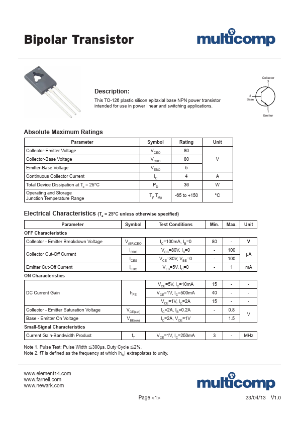
DESCRIPTION
: Collector 3 2 Base 1 Emitter ABSOLUTE MAXIMUM RATINGS
Parameter Collector-Emitter Voltage Collector-Base Voltage Emitter-Base Voltage Continuous Collector Current Total Device Dissipation at Tc = 25°C Operating and Storage Junction Temperature Range Symbol VCEO VCBO VEBO IC PD Tj, Tstg Rating 80 80 5 4 36 -65 to +150 ELECTRICAL CHARACTERISTICS
(Ta = 25°C unless otherwise specified) Parameter Symbol Test Conditions OFF Characteristics Collector - Emitter Breakdown Voltage Collector Cut-Off Current Emitter Cut-Off Current ON Characteristics V(BR)CEO ICBO ICES IEBO IC=100mA, IB=0 VCB=80V, IB=0 VCE=80V, VBE=0 VEB=5V, IC=0 DC Current Gain Collector - Emitter Saturation Voltage Base - Emitter On Voltage Small-Signal Characteristics hFE VCE(sat) VBE(on) VCE=5V, IC=10mA VCE=1V, IC=500mA VCE=1V, IC=2A IC=2A, IB=0.2A IC=2A, VCE=1V Current Gain-Bandwidth Product fT VCE=1V, IC=250mA Note 1. Pulse Test: Pulse Width %300μs, Duty Cycle %2%. Note 2. fT is defined as the frequency at which |hfe| extrapolates to unity. Multicomp