BD682
PNP Power Darlington Transistors
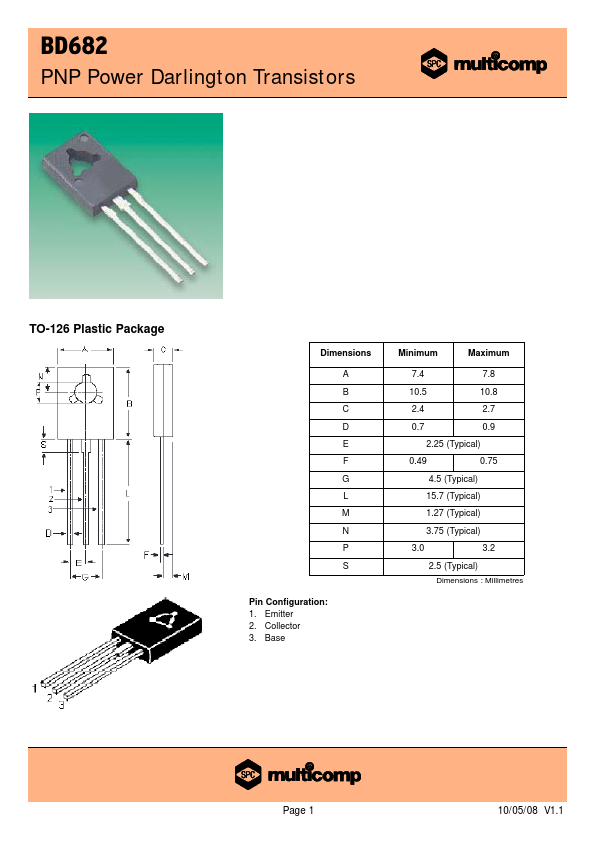
TO-126 Plastic Package
Dimensions
A B C D E F G L M N P S
Pin Configuration: 1. Emitter 2. Collector 3. Base
Minimum
Maximum
7.4 7.8 10.5 10.8 2.4 2.7 0.7 0.9
2.25 (Typical) 0.49 0.75
4.5 (Typical) 15.7 (Typical) 1.27 (Typical) 3.75 (Typical) 3.0 3.2 2.5 (Typical)
Dimensions : Millimetres
Page 1
10/05/08 V1.1
PNP Power Darlington Transistors
Absolute Maximum Ratings
Parameter
Symbol
Unit
Collector Base Voltage
Collector Emitter Voltage
Emitter Base Voltage
Collector Current
Base Current
Total Power Dissipation at Ta = 25°C Derate above 25°C Total Power Dissipation at TC = 25°C Derate above 25°C Operating and Storage Junction Temperature Range
VCBO VCEO VEBO
IC IB
Tj, Tstg
5.0 4.0 0.1 1.25 10 40 0.32
-55 to +150
W m W/°C
W W/°C
°C
Thermal Resistance
Junction to Case Junction to Ambient in Free Air
Rth (j-c) Rth (j-a)
3.13...