NCE7190
NCE7190 is N-Channel Enhancement Mode Power MOSFET manufactured by NCE Power.
Description
The NCE719 0 uses adv anced trenc h techno logy and design to provide excellent R DS(ON) with low gate charge. It can be used in a wide variety of applications.
General Features
- V DS = 71V,ID =90A RDS(ON) < 6.8mΩ @ VGS=10V ( Typ:5.9mΩ)
- Special process technology for high ESD capability
- High density cell design for ultra low Rdson
- Fully characterized avalanche voltage and current
- Good stability and uniformity with high EAS
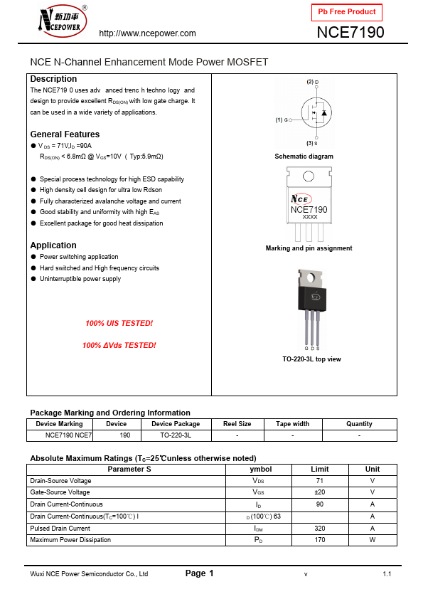
- Excellent package for good heat dissipation Schematic diagram
Application
- Power switching application
- Hard switched and High frequency circuits
- Uninterruptible power supply
Marking and pin assignment
100% UIS TESTED! 100% ΔVds TESTED!
TO-220-3L top view
Package Marking and Ordering Information
Device Marking NCE7190 NCE7 Device 190 Device Package TO-220-3L Reel Size Tape width Quantity
- Absolute Maximum Ratings (TC=25℃unless otherwise noted) Parameter S ymbol Drain-Source Voltage VDS Gate-Source Voltage VGS
Drain Current-Continuous Drain Current-Continuous(TC=100℃) I Pulsed Drain Current Maximum Power Dissipation
Limit
71 ±20 90 63 320 170
Unit
V V A A A W
D (100℃)
IDM PD
Wuxi NCE Power Semiconductor Co., Ltd
Page 1 v
1.1 http://..
Pb Free Product http://.ncepower.
Derating factor Single pulse avalanche energy (Note 5) Operating Junction and Storage Temperature Range EAS 550
1.13 W /℃ m J -55 To 175 ℃
TJ,TSTG
Thermal Characteristic
Thermal Resistance,Junction-to-Case (Note 2) RθJc 0.88 ℃/W
Electrical Characteristics (TC=25℃unless otherwise noted) Parameter Symbol Condition
Off Characteristics Drain-Source Breakdown Voltage Zero Gate Voltage Drain Current Gate-Body Leakage Current On Characteristics (Note 3) Gate Threshold Voltage Drain-Source On-State Resistance Forward Transconductance Dynamic Characteristics (Note4) Gate resistance Input Capacitance Output Capacitance Reverse Transfer Capacitance Switching Characteristics (Note 4) Turn-on Delay Time Turn-on Rise Time Turn-Off Delay...