2SD2163
2SD2163 is NPN Transistor manufactured by NEC.
FEATURES
- Mold package that does not require an insulating board or insulation bushing
- High DC current gain due to Darlington connection h FE = 1,000 MIN. (@IC = 10 A)
- Low collector saturation voltage: VCE(sat) = 1.5 V MAX. (@IC = 10 A)
ABSOLUTE MAXIMUM RATINGS (Ta = 25°C)
Parameter Collector to base voltage Collector to emitter voltage Emitter to base voltage Collector current (DC) Collector current (pulse) Base current (DC) Total power dissipation Total power dissipation Junction temperature Storage temperature Symbol VCBO VCEO VEBO IC(DC) IC(pulse)- IB(DC) PT (Tc = 25°C) PT (Ta = 25°C) Tj Tstg Ratings 150 100 8.0 ±10 ±20 1.0 30 2.0 150
- 55 to +150 Unit V V V A A A W W °C °C
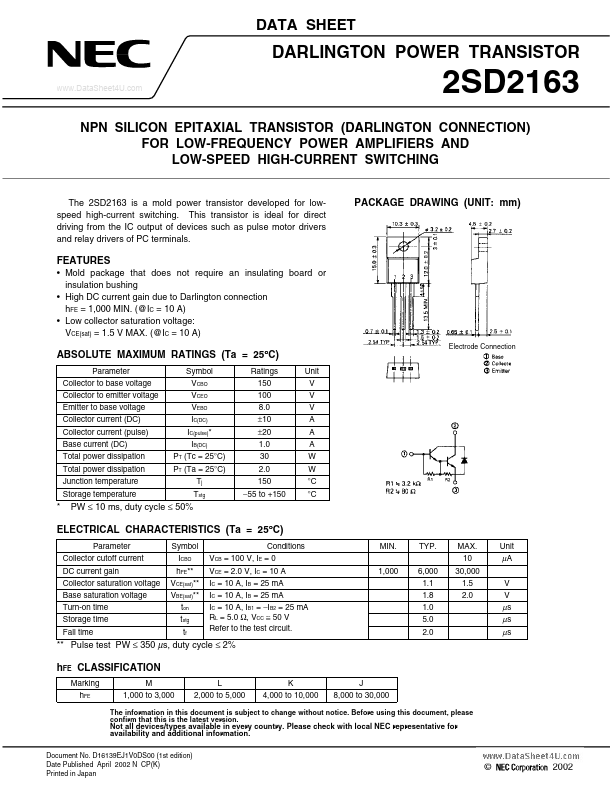
Electrode Connection
- PW ≤ 10 ms, duty cycle ≤ 50%
ELECTRICAL CHARACTERISTICS (Ta = 25°C)
Parameter Collector cutoff current DC current gain Collector saturation voltage Base saturation voltage Turn-on time Storage time Fall time Symbol ICBO h FE-
- VCE(sat)-
- VBE(sat)-
- ton tstg tf Conditions VCB = 100 V, IE = 0 VCE = 2.0 V, IC = 10 A IC = 10 A, IB = 25 m A IC = 10 A, IB = 25 m A IC = 10 A, IB1 =
- IB2 = 25 m A RL = 5.0 Ω, VCC ≅ 50 V Refer to the test circuit. 1,000 6,000 1.1 1.8 1.0 5.0 2.0 MIN. TYP. MAX. 10 30,000 1.5 2.0 Unit
µA
V V µs
µs µs
- - Pulse test PW ≤ 350 µs, duty cycle ≤ 2% h FE CLASSIFICATION
Marking h FE M 1,000 to 3,000 L 2,000 to 5,000 K 4,000 to 10,000 J 8,000 to 30,000
The information in this document is subject to change without notice. Before using this document, please confirm that this is the latest version.
Not all devices/types available in every country. Please check with local NEC representative for availability and additional information.
Document No. D16139EJ1V0DS00 (1st edition) Date Published April 2002 N CP(K) Printed in Japan
©
2002 1998
TYPICAL CHARACTERISTICS (Ta = 25°C)
..
Total Power Dissipation PT (W)
Case Temperature TC (°C)
Collector Current IC (A)
Collector to Emitter Voltage VCE (V)
Transient Thermal Resistance rth(j-c)(t)...