2SK2724
DESCRIPTION
This product is N-Channel MOS Field Effect Transistor designed for high current switching applications.
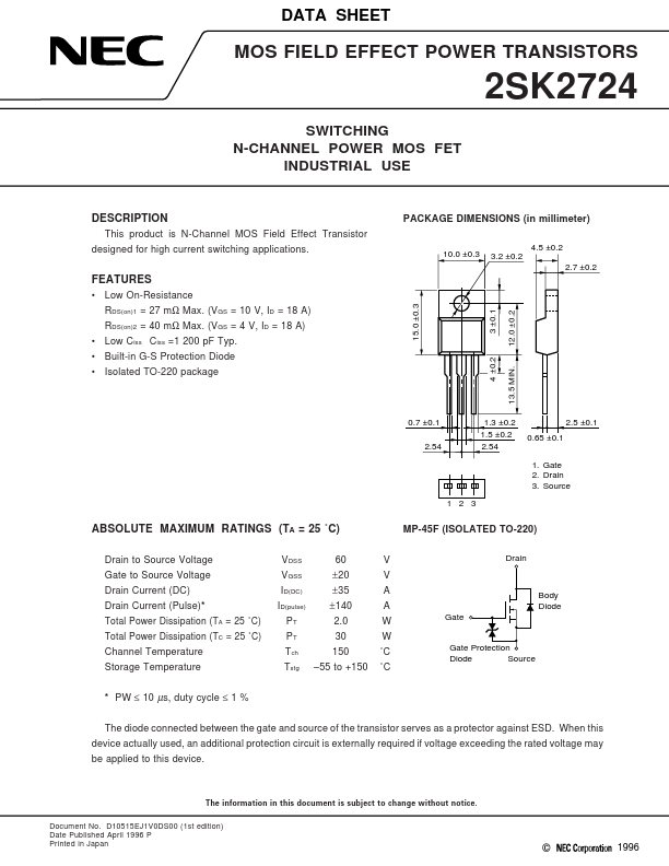
PACKAGE DIMENSIONS (in millimeter)
4.5 ±0.2 3.2 ±0.2 2.7 ±0.2
10.0 ±0.3
FEATURES
- Low On-Resistance
3 ±0.1 4 ±0.2 12.0 ±0.2 13.5 MIN.
RDS(on)1 = 27 mΩ Max. (VGS = 10 V, ID = 18 A) RDS(on)2 = 40 mΩ Max. (VGS = 4 V, ID = 18 A)
- Low Ciss Ciss =1 200 p F Typ.
- Built-in G-S Protection Diode
- Isolated TO-220 package
15.0 ±0.3
0.7 ±0.1 2.54
1.3 ±0.2 1.5 ±0.2 2.54
2.5 ±0.1 0.65 ±0.1 1. Gate 2. Drain 3. Source
1 2 3
ABSOLUTE MAXIMUM RATINGS (TA = 25 ˚C)
Drain to Source Voltage Gate to Source Voltage Drain Current (DC) Drain Current (Pulse)- Total Power Dissipation (TA = 25 ˚C) Total Power Dissipation (TC = 25 ˚C) Channel Temperature Storage Temperature
- PW ≤ 10 µs, duty cycle ≤ 1 % VDSS VGSS ID(DC) ID(pulse) PT PT Tch Tstg 60 ± 20 ± 35 ± 140 2.0 30 150
- 55 to +150 V V A A W W ˚C ˚C
MP-45F (ISOLATED TO-220)
Drain
Body Diode Gate
Gate Protection Diode Source
The...