2SK3355
2SK3355 is N-Channel MOSFET manufactured by NEC.
DESCRIPTION
The 2SK3355 is N-channel MOS Field Effect Transistor designed for high current switching applications.
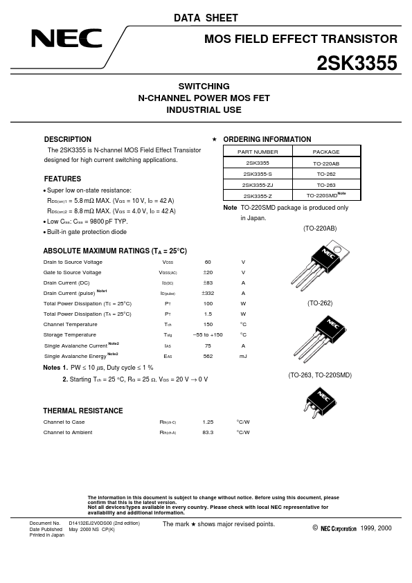
ORDERING INFORMATION
PART NUMBER 2SK3355 2SK3355-S 2SK3355-ZJ 2SK3355-Z PACKAGE TO-220AB TO-262 TO-263 TO-220SMDNote
FEATURES
- Super low on-state resistance: RDS(on)1 = 5.8 mΩ MAX. (VGS = 10 V, ID = 42 A) RDS(on)2 = 8.8 mΩ MAX. (VGS = 4.0 V, ID = 42 A)
- Low Ciss: Ciss = 9800 p F TYP.
- Built-in gate protection diode
Note TO-220SMD package is produced only in Japan. (TO-220AB)
ABSOLUTE MAXIMUM RATINGS (TA = 25°C)
Drain to Source Voltage Gate to Source Voltage Drain Current (DC) Drain Current (pulse)
Note1
VDSS VGSS(AC) ID(DC) ID(pulse) PT PT Tch Tstg
Note2 Note2
60 ±20 ±83 ±332 100 1.5 150
- 55 to +150 75 562
V V A A W W °C °C A m J
Total Power Dissipation (TC = 25°C) Total Power Dissipation (TA = 25°C) Channel Temperature Storage Temperature Single Avalanche Current Single Avalanche Energy
(TO-262)
IAS EAS
Notes 1. PW ≤ 10 µs, Duty cycle ≤ 1 % 2. Starting Tch = 25 °C, RG = 25 Ω, VGS = 20 V → 0 V (TO-263, TO-220SMD)
THERMAL RESISTANCE
Channel to Case Channel to Ambient Rth(ch-C) Rth(ch-A) 1.25 83.3 °C/W °C/W
The information in this document is subject to change without notice. Before using this document, please confirm that this is the latest version.
Not all devices/types available in every country. Please check with local NEC representative for availability and additional information.
Document No. D14132EJ2V0DS00 (2nd edition) Date Published May 2000 NS CP(K) Printed in Japan
The mark 5 shows major revised points.
©
1999, 2000
ELECTRICAL CHARACTERISTICS (TA = 25 °C)
CHARACTERISTICS Drain to Source On-state Resistance SYMBOL RDS(on)1 RDS(on)2 Gate to Source Cut-off Voltage Forward Transfer Admittance Drain Leakage Current Gate to Source Leakage Current Input Capacitance Output Capacitance Reverse Transfer Capacitance Turn-on Delay Time Rise Time Turn-off Delay Time Fall Time Total Gate Charge Gate to Source Charge Gate to Drain...