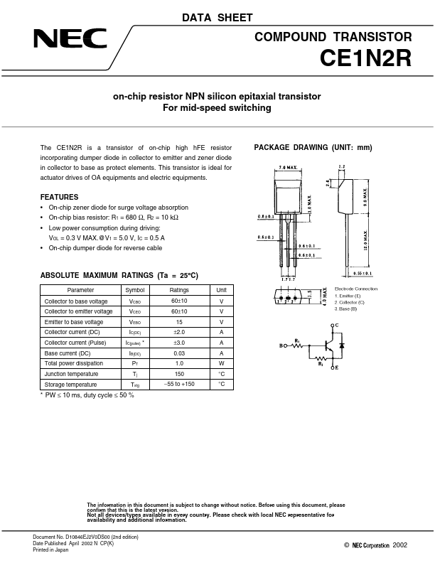
• Part: CE1N2R
  • Description: on-chip resistor NPN silicon epitaxial transistor
  • Category: Transistor
  • Manufacturer: NEC
  • Size: 54.27 KB
Download CE1N2R Datasheet PDF
NEC
CE1N2R
CE1N2R is on-chip resistor NPN silicon epitaxial transistor manufactured by NEC.
FEATURES - On-chip zener diode for surge voltage absorption - On-chip bias resistor: R1 = 680 Ω, R2 = 10 kΩ - Low power consumption during driving: VOL = 0.3 V MAX.@V1 = 5.0 V, IC = 0.5 A - On-chip dumper diode for reverse cable ABSOLUTE MAXIMUM RATINGS (Ta = 25°C) Parameter Collector to base voltage Collector to emitter voltage Emitter to base voltage Collector current (DC) Collector current (Pulse) Base current (DC) Total power dissipation Junction temperature Storage temperature Symbol VCBO VCEO VEBO IC(DC) IC(pulse) - IB(DC) PT Tj Tstg Ratings 60±10 60±10 15 ±2.0 ±3.0 0.03 1.0 150 - 55 to +150 Unit V V V A A A W °C °C - PW ≤ 10 ms, duty cycle ≤ 50 % The information in this document is subject to change without notice. Before using this document, please confirm that this is the latest version. Not all devices/types available in every country. Please check with local NEC representative for availability and additional information. Document No. D10846EJ2V0DS00 (2nd edition) Date Published April 2002 N CP(K) Printed in Japan © 2002 1998 ELECTRICAL CHARACTERISTICS (Ta = 25°C) Parameter Colletor to emitter voltage Collector cutoff current DC current gain DC current gain DC current gain Low level output voltage Low level input voltage Input resistance E-to-B resistance Turn-on time Storage time Fall time Symbol VCEO(SUS) ICBO h FE1 - - h FE2 - - h FE3 - - VOL - - VIL - - R1 R2 ton tstg tf IC = 1.0 A IBI = - IB2 = 10 m A VCC = 20 V, RL = 20 Ω Conditions IC = 2.0 A, IB = 5.0 m A, L = 6.0 m H VCB = 40 V, IE = 0 VCE = 5.0 V, IC = 0.2 A VCE = 5.0 V, IC = 1.0 A VCE = 5.0 V, IC = 2.0 A VI = 5.0 V, IC = 0.5 A VCE = 12 V, IC = 100 µA 476 7.0 700 1000 500 1200 1700 1300 0.12 0.43 680 10.0 0.4 1.4 0.5 0.3 0.4 884 13.0 3000 MIN. 50 TYP. 60 100 MAX. Unit V n A - - - V V Ω kΩ µs µs µs - - Pulse test PW ≤ 350 µs, duty cycle ≤ 2 % REMENDED SOLDERING CONDITIONS This product should be soldered and mounted under the following remended conditions. For soldering methods and conditions...