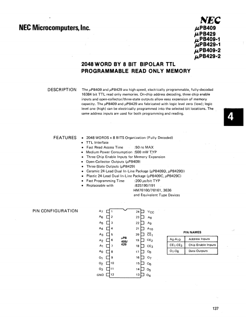
Datasheet Summary
NEe Microputers, Inc.
NEe p.PB409
J'!PB429 ",PB409-1 }LPB429-1 p.PB409-2
ILPB429-2
2048 WORD BY 8 BIT BIPOLAR TTL
PROGRAMMABLE READ ONLY MEMORY
DESC RIPT ION
The JlPB409 and JlPB429 are high-speed, electrically programmable, fully-decoded 16384 bit TTL read only memories. On-chip address decoding, three chip enable inputs and open-collector/three-state outputs allow easy expansion of memory capacity. The JlPB409 and JlPB429 are fabricated with logic level zero (low); logic level one (high) can be electrically programmed into the selected bit locations. The . same address inputs are used for both programming and reading.
Features
- 2048 WORDS x 8 BITS Organization (Fully Decoded)
-...