The following content is an automatically extracted verbatim text
from the original manufacturer datasheet and is provided for reference purposes only.
View original datasheet text
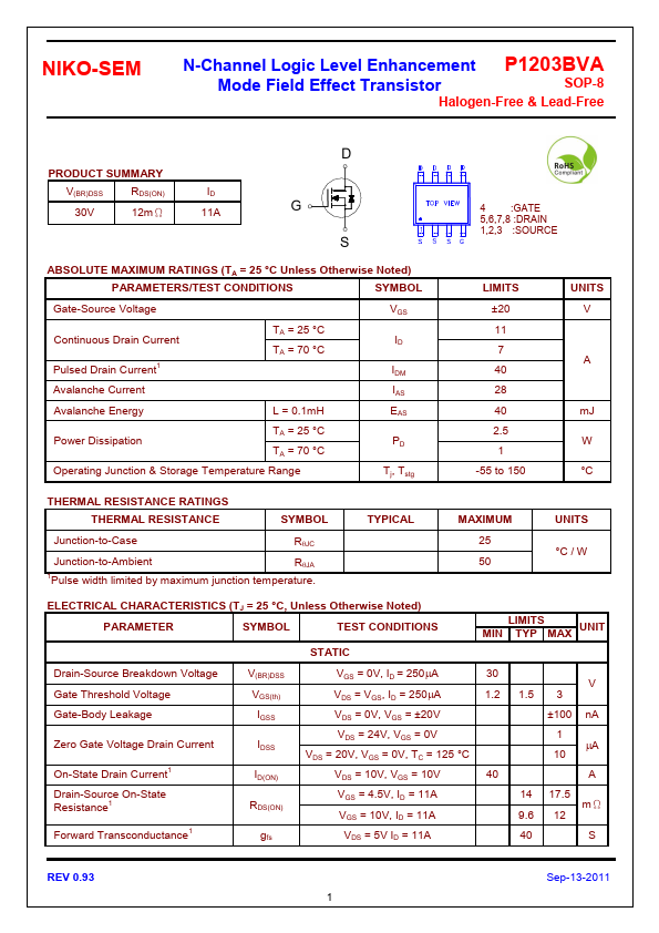
NIKO-SEM
N-Channel Logic Level Enhancement P1203BVA
Mode Field Effect Transistor
SOP-8
Halogen-Free & Lead-Free
PRODUCT SUMMARY
V(BR)DSS
RDS(ON)
30V
12mΩ
ID 11A
D
G S
4 :GATE 5,6,7,8 :DRAIN 1,2,3 :SOURCE
ABSOLUTE MAXIMUM RATINGS (TA = 25 °C Unless Otherwise Noted)
PARAMETERS/TEST CONDITIONS
SYMBOL
Gate-Source Voltage
Continuous Drain Current Pulsed Drain Current1
TA = 25 °C TA = 70 °C
Avalanche Current
Avalanche Energy
L = 0.1mH
Power Dissipation
TA = 25 °C TA = 70 °C
Operating Junction & Storage Temperature Range
VGS ID IDM IAS EAS PD Tj, Tstg
LIMITS ±20 11 7 40 28 40 2.5 1
-55 to 150
UNITS V
A
mJ W °C
THERMAL RESISTANCE RATINGS THERMAL RESISTANCE
SYMBOL
Junction-to-Case
RθJC
Junction-to-Ambient
RθJA
1Pulse width limited by maximum junction temperature.