Datasheet4U.com
🌙
P1606BT Datasheet | NIKO-SEM
Part:
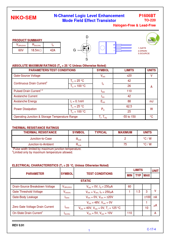
P1606BT
Description:
N-Channel Transistor
Category:
Transistor
Manufacturer:
NIKO-SEM
Size:
626.95 KB
P1606BT Datasheet (PDF) Download
Related P1606BT Datasheets
P1604ES P-Channel Field Effect Transistor
P1604ETF P-Channel Field Effect Transistor
NIKO-SEM
P1606BT
×
Close