P1820HTFB
Description
NIKO-SEM N-Channel Enhancement Mode P1820HTFB Field Effect Transistor TO-220F Halogen-Free & Lead-Free PRODUCT SUMMARY V(BR)DSS RDS(ON) 200V 150mΩ ID 18A D G S ABSOLUTE MAXIMUM RATINGS (...
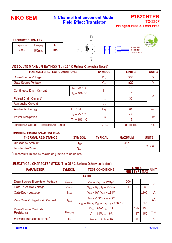
NIKO-SEM N-Channel Enhancement Mode P1820HTFB Field Effect Transistor TO-220F Halogen-Free & Lead-Free PRODUCT SUMMARY V(BR)DSS RDS(ON) 200V 150mΩ ID 18A D G S ABSOLUTE MAXIMUM RATINGS (...
| Part Number | Manufacturer | Description |
|---|---|---|
| P1820HTFB | UNIKC | N-Channel MOSFET |
| P1820HDB | UNIKC | N-Channel MOSFET |
| P1820BD | UNIKC | N-Channel Transistor |
| P1825AT | UNIKC | N-Channel MOSFET |
| P1825HTFB | UNIKC | N-Channel MOSFET |
| P1825AD | UNIKC | N-Channel Transistor |
| P1821 | Alliance Semiconductor | Low Power Mobile VGA EMI Reduction IC |
| P1825HDB | UNIKC | N-Channel MOSFET |
| P1818 | Alliance Semiconductor | Low Power Mobile VGA EMI Reduction IC |