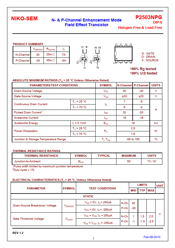
P2503NPG Overview
| Part | P2503NPG |
|---|---|
| Description | N- & P-Channel Field Effect Transistor |
| Category | Transistor |
| Manufacturer | NIKO-SEM |
| Size | 475.99 KB |
| Part Number | Manufacturer | Description |
|---|---|---|
| P2503NVG | UNIKC | N&P-Channel MOSFET |
| P2503HVG | UNIKC | N-Channel MOSFET |
| P2503BDG | UNIKC | N-Channel MOSFET |
| P2503HEA | UNIKC | MOSFET |
| P2500M | Taiwan Semiconductor | Glass Passivated Rectifier |