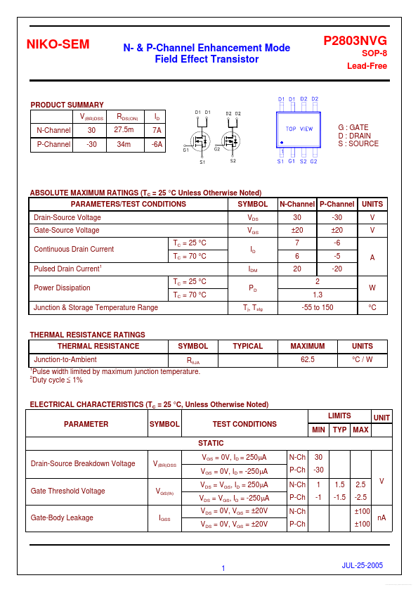
Datasheet4U Logo Datasheet4U.com

P2803NVG - N-&P-Channel MOSFET

Download the P2803NVG datasheet PDF. This datasheet also covers the P2803NVG_NIKO variant, as both devices belong to the same n-&p-channel mosfet family and are provided as variant models within a single manufacturer datasheet.

📥 Download Datasheet

Note: The manufacturer provides a single datasheet file (P2803NVG_NIKO-SEM.pdf) that lists specifications for multiple related part numbers.

Full PDF Text Transcription (Reference)

The following content is an automatically extracted verbatim text from the original manufacturer datasheet and is provided for reference purposes only.

View original datasheet text
NIKO-SEM N- & P-Channel Enhancement Mode Field Effect Transistor P2803NVG SOP-8 Lead-Free PRODUCT SUMMARY V(BR)DSS N-Channel P-Channel 30 -30 RDS(ON) 27.5m 34m ID 7A -6A G : GATE D : DRAIN S : SOURCE ABSOLUTE MAXIMUM RATINGS (TC = 25 °C Unless Otherwise Noted) PARAMETERS/TEST CONDITIONS Drain-Source Voltage Gate-Source Voltage Continuous Drain Current Pulsed Drain Current Power Dissipation Junction & Storage Temperature Range 1 SYMBOL VDS VGS N-Channel P-Channel 30 ±20 7 6 20 2 1.3 -55 to 150 -30 ±20 -6 -5 -20 UNITS V V TC = 25 °C TC = 70 °C ID IDM A TC = 25 °C TC = 70 °C PD Tj, Tstg W °C THERMAL RESISTANCE RATINGS THERMAL RESISTANCE Junction-to-Ambient 1 2 SYMBOL RθJA TYPICAL MAXIMUM 62.5 UNITS °C / W Pulse width limited by maximum junction temperature.