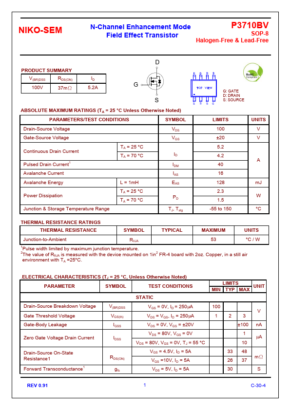
P3710BV Overview
| Part | P3710BV |
|---|---|
| Description | N-Channel Enhancement Mode Field Effect Transistor |
| Category | Transistor |
| Manufacturer | NIKO-SEM |
| Size | 221.67 KB |
| Part Number | Manufacturer | Description |
|---|---|---|
| P3710BV | UNIKC | N-Channel MOSFET |
| P3710BTF | UNIKC | N-Channel MOSFET |
| P3710BD | VBsemi | N-Channel 100V MOSFET |
| P3710BT | UNIKC | N-Channel MOSFET |
| P3710BD | UNIKC | N-Channel Transistor |