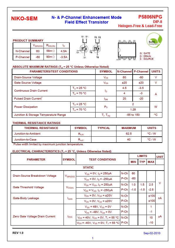
Download the P5806NPG datasheet PDF.
This datasheet also covers the P5806NPG-NIKO variant, as both devices belong to the same n- & p-channel field effect transistor family and are provided as variant models within a single manufacturer datasheet.
Full PDF Text Transcription for P5806NPG (Reference)
Note: Below is a high-fidelity text extraction (approx. 800 characters) for
P5806NPG. For precise diagrams, and layout, please refer to the original PDF.
Free PRODUCT SUMMARY V(BR)DSS RDS(ON) N-Channel 60 58mΩ P-Channel -60 90mΩ ID 4.5A -3.5A D1 D1 D2 D2 #1S1 G1 S2 G2 G : GATE D : DRAIN S : SOURCE ABSOLUTE MAXIMUM RATINGS (TA = 25 °C Unless Otherwise Noted) PARAMETERS/TEST CONDITIONS SYMBOL Drain-Source Voltage Gate-Source Voltage Continuous Drain Current Pulsed Drain Current1 Power Dissipation Junction & Storage Temperature Range TA = 25 °C TA = 70 °C TA = 25 °C TA = 70 °C VDS VGS ID IDM PD Tj, Tstg N-Channel P-Channel UNITS 60 -60 V ±20 ±20 V 4.5 -3.5 4 -3 A 20 -20 2 W 1.