P6006BI
Overview
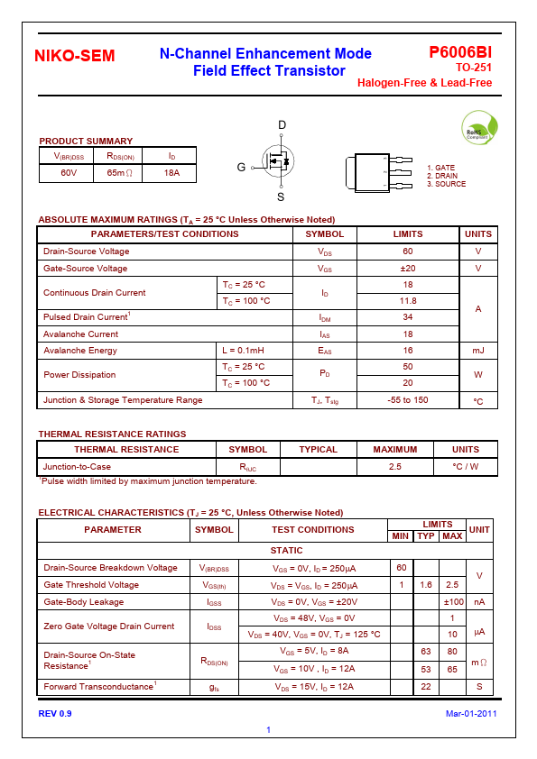
NIKO-SEM N-Channel Enhancement Mode P6006BI Field Effect Transistor TO-251 Halogen-Free & Lead-Free PRODUCT SUMMARY V(BR)DSS RDS(ON) 60V 65mΩ ID 18A D G S ABSOLUTE MAXIMUM RATINGS (TA = 2...
| Part | P6006BI |
|---|---|
| Description | N-Channel Transistor |
| Category | Transistor |
| Manufacturer | NIKO-SEM |
| Size | 241.21 KB |
NIKO-SEM N-Channel Enhancement Mode P6006BI Field Effect Transistor TO-251 Halogen-Free & Lead-Free PRODUCT SUMMARY V(BR)DSS RDS(ON) 60V 65mΩ ID 18A D G S ABSOLUTE MAXIMUM RATINGS (TA = 2...
| Part Number | Manufacturer | Description |
|---|---|---|
| P6006BI | UNIKC | N-Channel MOSFET |
| P6006BD | UNIKC | N-Channel Transistor |
| P6006HV | UNIKC | Dual N-Channel MOSFET |
| P600D | Good-Ark Semiconductor | GENERAL PURPOSE PLASTIC RECTIFIER |
| P600B | Good-Ark Semiconductor | GENERAL PURPOSE PLASTIC RECTIFIER |