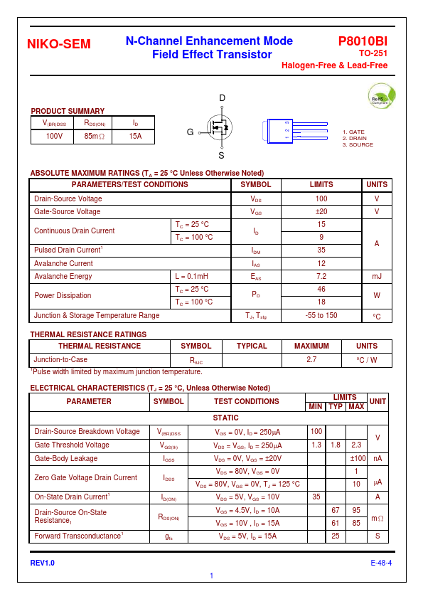
Datasheet4U Logo Datasheet4U.com

P8010BI - N-Channel Enhancement Mode Field Effect Transistor

Download the P8010BI datasheet PDF. This datasheet also covers the P8010BI-NIKO variant, as both devices belong to the same n-channel enhancement mode field effect transistor family and are provided as variant models within a single manufacturer datasheet.

📥 Download Datasheet

Note: The manufacturer provides a single datasheet file (P8010BI-NIKO-SEM.pdf) that lists specifications for multiple related part numbers.

Datasheet Details

Part number P8010BI
Manufacturer NIKO-SEM
File Size 303.46 KB
Description N-Channel Enhancement Mode Field Effect Transistor
Datasheet download datasheet P8010BI Datasheet

Full PDF Text Transcription (Reference)

The following content is an automatically extracted verbatim text from the original manufacturer datasheet and is provided for reference purposes only.

View original datasheet text
NIKO-SEM N-Channel Enhancement Mode P8010BI Field Effect Transistor TO-251 Halogen-Free & Lead-Free PRODUCT SUMMARY V(BR)DSS RDS(ON) 100V 85mΩ ID 15A D G S 12 3 1. GATE 2. DRAIN 3. SOURCE ABSOLUTE MAXIMUM RATINGS (TA = 25 °C Unless Otherwise Noted) PARAMETERS/TEST CONDITIONS SYMBOL Drain-Source Voltage Gate-Source Voltage Continuous Drain Current Pulsed Drain Current1 Avalanche Current Avalanche Energy Power Dissipation Junction & Storage Temperature Range TC = 25 °C TC = 100 °C L = 0.1mH TC = 25 °C TC = 100 °C VDS VGS ID IDM IAS EAS PD TJ, Tstg LIMITS 100 ±20 15 9 35 12 7.2 46 18 -55 to 150 UNITS V V A mJ W °C THERMAL RESISTANCE RATINGS THERMAL RESISTANCE SYMBOL Junction-to-Case RJC 1Pulse width limited by maximum junction temperature. TYPICAL MAXIMUM 2.