Datasheet4U.com
🌙
PB555BA Datasheet | NIKO-SEM
Part:
PB555BA
Description:
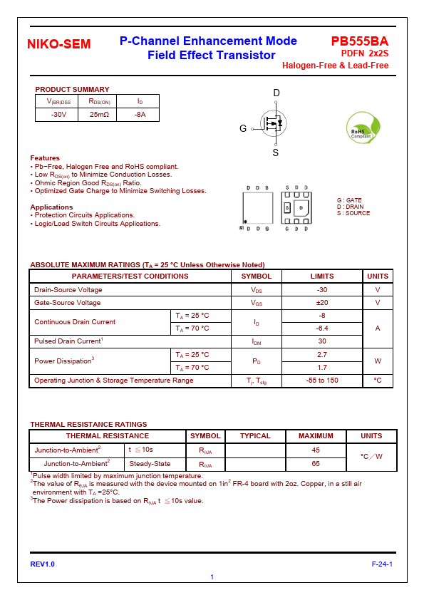
P-Channel Enhancement Mode Field Effect Transistor
Category:
Transistor
Manufacturer:
NIKO-SEM
Size:
248.64 KB
PB555BA Datasheet (PDF) Download
NIKO-SEM
PB555BA
Key Features
Pb-Free, Halogen Free and RoHS compliant.
Low RDS(on) to Minimize Conduction Losses.
Ohmic Region Good RDS(on) Ratio.
Optimized Gate Charge to Minimize Switching Losses.
Datasheets by Manufacturer
PB555BA
— UNIKC — P-Channel MOSFET
PB554DY
— UNIKC — MOSFET
×
Close