PI5B3BA
PI5B3BA is P-Channel Enhancement Mode Field Effect Transistor manufactured by NIKO-SEM.
- Part of the PI5B3BA-NIKO comparator family.
- Part of the PI5B3BA-NIKO comparator family.
Features
- Pb- Free, Halogen Free and Ro HS pliant.
- Low RDS(on) to Minimize Conduction Losses.
- Ohmic Region Good RDS(on) Ratio.
- Optimized Gate Charge to Minimize Switching Losses.
Applications
- Protection Circuits Applications.
- Logic/Load Switch Circuits Applications.
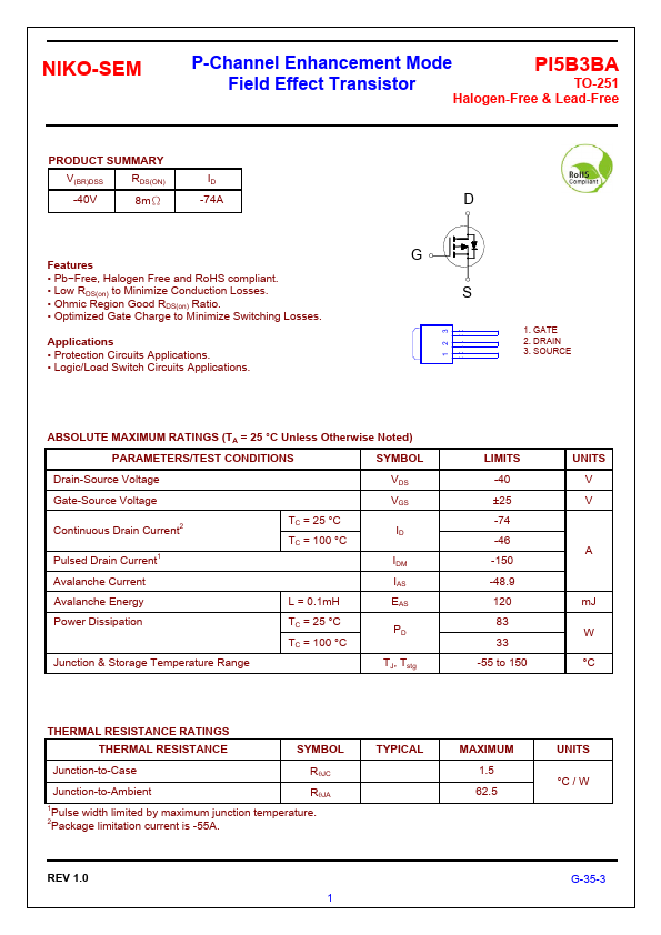
12 3
1. GATE 2. DRAIN 3. SOURCE
ABSOLUTE MAXIMUM RATINGS (TA = 25 °C Unless Otherwise Noted)
PARAMETERS/TEST CONDITIONS
SYMBOL
Drain-Source Voltage Gate-Source Voltage Continuous Drain Current2 Pulsed Drain Current1 Avalanche Current Avalanche Energy Power Dissipation
Junction & Storage Temperature Range
TC = 25 °C TC = 100 °C
L = 0.1m H TC = 25 °C TC = 100 °C
VDS VGS
IDM IAS EAS PD
TJ, Tstg
LIMITS -40 ±25 -74 -46 -150 -48.9 120 83 33
-55 to 150
UNITS V V
A m J W °C
THERMAL RESISTANCE RATINGS THERMAL RESISTANCE
SYMBOL
Junction-to-Case
RJC
Junction-to-Ambient
RJA
1Pulse width limited by maximum junction temperature. 2Package limitation current is -55A.
TYPICAL
MAXIMUM 1.5 62.5
UNITS °C / W
REV 1.0
G-35-3
NIKO-SEM...