17529
17529 is dual H-Bridge motor driver manufactured by NXP Semiconductors.
features an on-board charge pump, as well as built-in shoot-through current protection and an undervoltage shutdown function. The 17529 has four operating modes: forward, reverse, brake, and tri-stated (high-impedance). The 17529 has a low total RDS(on) of 1.2 Ω (max at 25 °C). The 17529’s low output resistance and high slew rate provides efficient drive for many types of micromotors.
Features
- Low total RDS(on) 0.7 Ω (typ), 1.2 Ω (max) at 25 °C
- Output current 0.7 A (DC), 1.4 A (peak)
- Shoot-through current protection circuit
- 3.0 V/5.0 V CMOS-patible inputs
- PWM control input frequency up to 200 k Hz
- Built-in charge pump circuit
- Low power consumption
- Undervoltage detection and shutdown circuit
Document Number: MPC17529 Rev. 4.0, 7/2016
DUAL H-BRIDGE
EV SUFFIX (PB-FREE) 98ASA10616D 20-PIN VMFP
EJ SUFFIX (PB-FREE) 98ASA00887D 20-PIN TSSOP
WITH EXPOSED PAD
5.0 V
5.0 V
VDD VM 1/2
C1L
C1H
C2L C2H
OUT1A
CRES OUT1B
IN1A OUT2A
Bipolar
IN1B IN2A
OUT2B
N Step
Motor
IN2B
GND PGND1/2
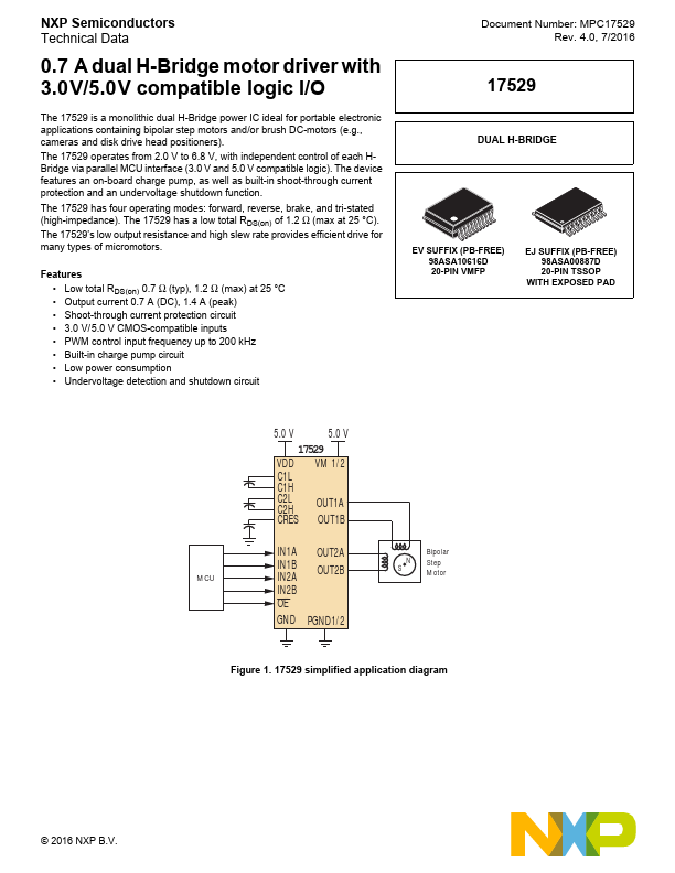
Figure 1. 17529 simplified application diagram
© 2016 NXP B.V.
ORDERABLE PARTS
Orderable...