FEATURES
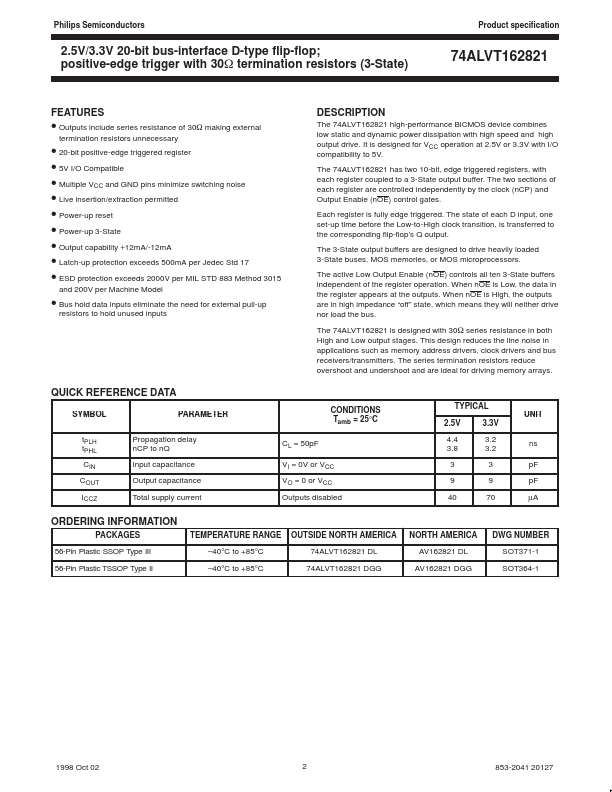
● Outputs include series resistance of 30W making external termination resistors unnecessary DESCRIPTION
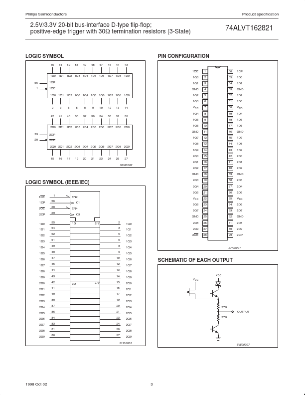
The two sections of each register are controlled independently by the clock (nCP) and Output Enable (nOE) control gates. Each register is fully edge triggered. The state of each D input, one set-up time before the Low-to-High clock transition, is transferred to the corresponding flip-flop’s Q output. The 3-State output buffers are designed to drive heavily loaded 3-State buses, MOS memories, or MOS microprocessors. The active Low Output Enable (nOE) controls all ten 3-State buffers independent of the register operation. When nOE is Low, the data in the register appears at the outputs. When nOE is High, the outputs are in high impedance “off” state, which means they will neither drive nor load the bus. The 74ALVT162821 is designed with 30W series resistance in both High and Low output stages. This design reduces the line noise in applications such as memory address drivers, clock drivers and bus receivers/transmitters. NXP Semiconductors