NXP Semiconductors 74AUP2G79
The 74AUP2G79 is a high-performance, low-power, low-voltage, Si-gate CMOS device, superior to most advanced CMOS compatible TTL families. This device ensures a very low static and dynamic power consumption across the entire VCC range from 0.8 V to 3.6 V. This device is fully specified for partial power-down applications using IOFF.| Part No. | 74AUP2G79 |
|---|---|
| Datasheet | 74AUP2G79 Download |
| Manufacturer |  NXP Semiconductors |
| Description | Low-power dual D-type flip-flop |
| Buy | Stock & Price |
FEATURES
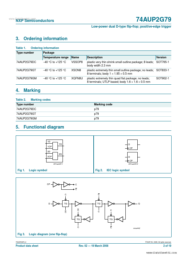
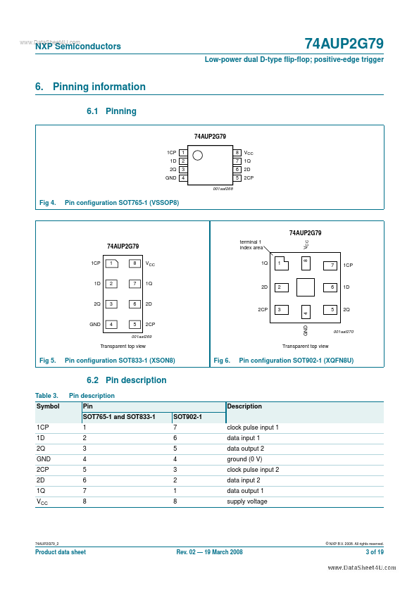
I Wide supply voltage range from 0.8 V to 3.6 V I High noise immunity I Complies with JEDEC standards: N JESD8-12 (0.8 V to 1.3 V) N JESD8-11 (0.9 V to 1.65 V) N JESD8-7 (1.2 V to 1.95 V) N JESD8-5 (1.8 V to 2.7 V) N JESD8-B (2.7 V to 3.6 V) I ESD protection: N HBM JESD22-A114E Class 3A exceeds 5000 V N MM JESD22-A115-A exceeds 200 V N CDM JESD22-C101-C exceeds 1000 V I Low static power consumption; ICC = 0.9 µA (maximum) I Latch-up performance exceeds 100 mA per JESD78 Class II I Inputs accept voltages up to 3.6 V I Low noise overshoot and undershoot < 10 % of VCC I IOFF circuitry provides partial Power-down mode operation I Multiple package options I Specified from −40 °C to +85 °C and −40 °C to +125 °C NXP Semiconductors 74AUP2G79 Low-power dual D-type flip-flop; positive-edge trigger 3. Ordering information Table 1. Ordering information Package Temperature range Name 74AUP2G79DC 74AUP2G79GT 74AUP2G79GM −40 °C to +125 °C −40 °C to +125 °C −40 °C to +125 °C VSSOP8 XSON8 XQFN8U...