NXP Semiconductors 74LVC377
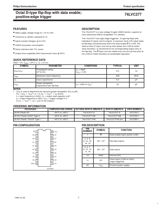
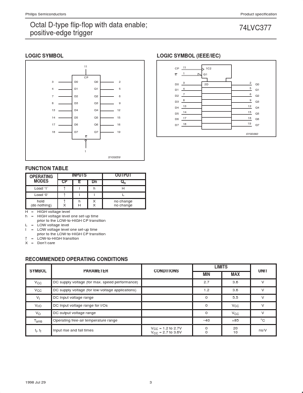
The 74LVC377 is a low-voltage Si-gate CMOS device, superior to most advanced CMOS compatible TTL families. The 74LVC377 has eight edge-triggered , D-type flip-flops with individual D inputs and Q outputs. The state of each D input, one set-up time before the LOW-to-HIGH clock transition, is transferred to the corresponding output (Qn) of the flip-flop.| Part No. | 74LVC377 |
|---|---|
| Datasheet | 74LVC377 Download |
| Manufacturer |  NXP Semiconductors |
| Description | Octal D-type flip-flop |
| Buy | Stock & Price |
FEATURES
● Wide supply voltage range of 1.2V to 3.6V● Conforms to JEDEC standard 8-1A
● Inputs accept voltages up to 5.5V
● CMOS low power consumption
● Direct interface with TTL levels
● Output drive capability 50Ω transmission lines @ 85°C QUICK REFERENCE DATA GND = 0V; Tamb = 25°C; tr =tf v2.5 ns SYMBOL tPHL/tPLH fmax CI CPD PARAMETER Propagation delay CP to Qn; Maximum clock frequency Input capacitance Power dissipation capacitance per flip-flop
DESCRIPTION
A common clock (CP) input loads all flip-flops simultaneously when the data enable E is LOW. The E input must be stable only one set-up time prior to the LOW-to-HIGH transition for predictable operation. CONDITIONS CL = 50pF VCC = 3.3V TYPICAL 6.0 230 5.0 UNIT ns MHz pF pF VI = GND to VCC1 22 NOTES: 1 CPD is used to determine the dynamic power dissipation (PD in µW) VCC2 x fi )S (CL VCC2 fo) where: PD = CPD fi = input frequency in MHz; CL = output load capacity in pF; fo = output frequency in MHz; VCC = supply voltage in V; VCC2 fo) = sum of the outputs.