NXP Semiconductors 74LVC3G07
The 74LVC3G07 is a high-performance, low-power, low-voltage, Si-gate CMOS device and superior to most advanced CMOS compatible TTL families. This feature allows the use of this device in a mixed 3.3 V and 5 V environment. This device is fully specified for partial power-down applications using Ioff.| Part No. | 74LVC3G07 |
|---|---|
| Datasheet | 74LVC3G07 Download |
| Manufacturer |  NXP Semiconductors |
| Description | Triple buffer |
| Buy | Stock & Price |
FEATURES
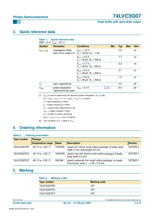
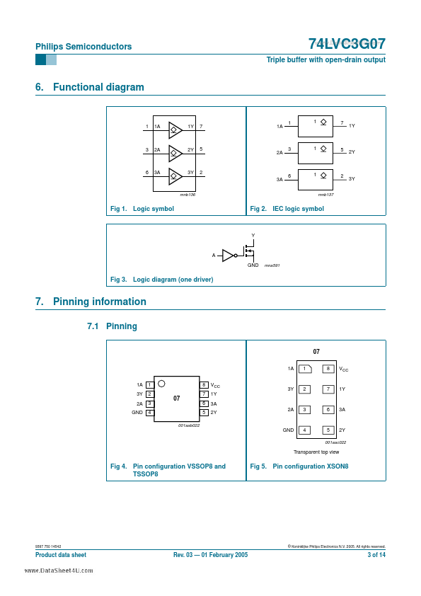
s s s s Wide supply voltage range from 1.65 V to 5.5 V 5 V tolerant input/output for interfacing with 5 V logic High noise immunity Complies with JEDEC standard: x JESD8-7 (1.65 V to 1.95 V) x JESD8-5 (2.3 V to 2.7 V) x JESD8-B/JESD36 (2.7 V to 3.6 V). ESD protection: x HBM EIA/JESD22-A114-B exceeds 2000 V x MM EIA/JESD22-A115-A exceeds 200 V. −24 mA output drive (VCC = 3.0 V) CMOS low power consumption Latch-up performance exceeds 250 mA Direct interface with TTL levels Inputs accept voltages up to 5 V Multiple package options Specified from −40 °C to +85 °C and −40 °C to +125 °C. s s s s s s s s Philips Semiconductors 74LVC3G07 Triple buffer with open-drain output 3. Quick reference data Table 1: Quick reference data GND = 0 V; Tamb = 25 °C. Symbol tPLZ, tPZL Parameter Conditions Min [1] [2] Typ 2.9 1.7 2.3 2.1 1.5 2.5 6.5 Max - Unit ns ns ns ns ns pF pF propagation delay VCC = 1.8 V; input nA to output nY CL = 30 pF; RL = 1 kΩ VCC = 2.5 V; CL = 30 pF; RL = 500 Ω VCC = 2.7 V;...