Datasheet Summary
Triple buffer with open-drain output
Rev. 14
- 28 January 2021
Product data sheet
1. General description
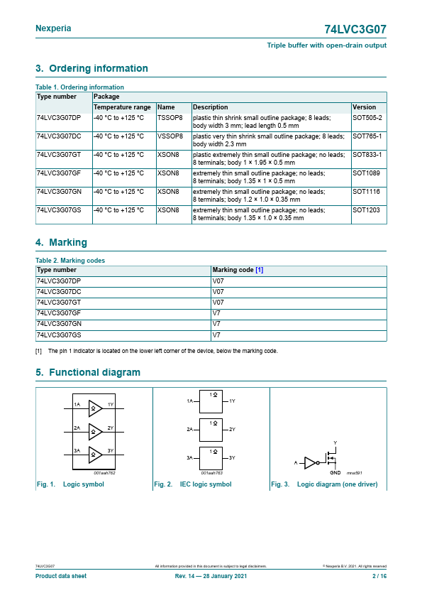
The 74LVC3G07 provides three non-inverting buffers.
The output of the device is an open-drain and can be connected to other open-drain outputs to implement active-LOW wired-OR or active-HIGH wired-AND functions.
Input can be driven from either 3.3 V or 5 V devices. This feature allows the use of this device in a mixed 3.3 V and 5 V environment.
Schmitt trigger action at all inputs makes the circuit tolerant for slower input rise and fall time.
This device is fully specified for partial power-down applications using IOFF. The IOFF circuitry disables the output, preventing the...