NXP Semiconductors A2I09VD030N
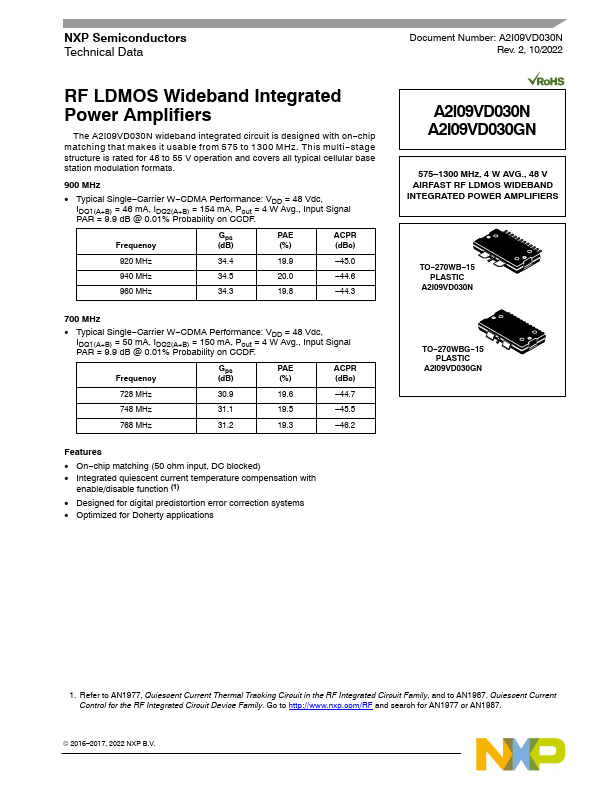
The A2I09VD030N wideband integrated circuit is designed with on−chip matching that makes it usable from 575 to 1300 MHz. This multi−stage structure is rated for 48 to 55 V operation and covers all typical cellular base station modulation formats.| Part No. | A2I09VD030N |
|---|---|
| Datasheet | A2I09VD030N Download |
| Manufacturer |  NXP Semiconductors |
| Description | Power Amplifiers |
| Buy | Stock & Price |
FEATURES
● On−chip matching (50 ohm input, DC blocked)● Integrated quiescent current temperature compensation with enable/disable function (1)
● Designed for digital predistortion error correction systems
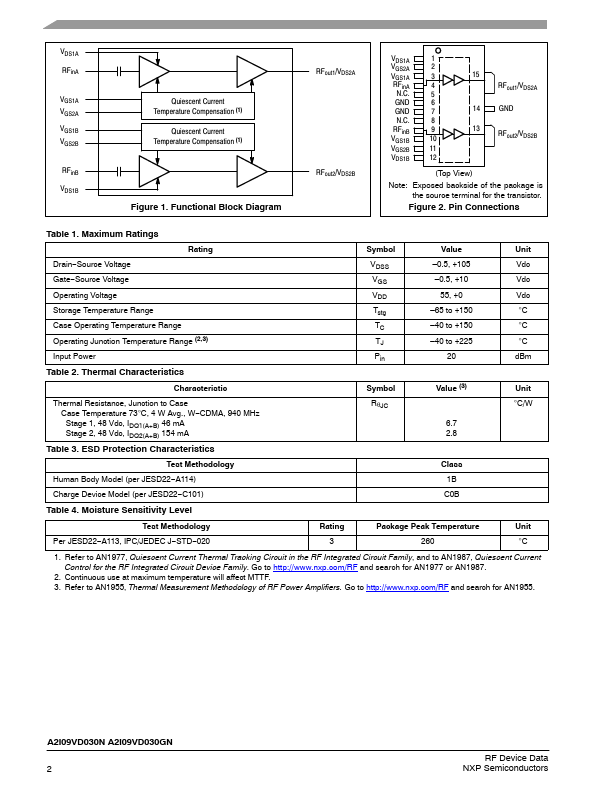
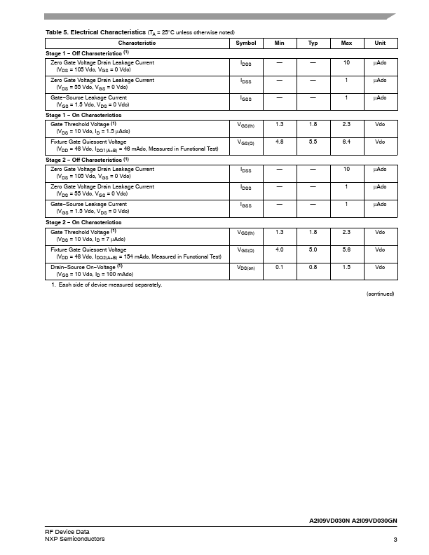
● Optimized for Doherty applications A2I09VD030N A2I09VD030GN 575–1300 MHz, 4 W AVG., 48 V AIRFAST RF LDMOS WIDEBAND INTEGRATED POWER AMPLIFIERS TO−270WB−15 PLASTIC A2I09VD030N TO−270WBG−15 PLASTIC A2I09VD030GN 1. Refer to AN1977, Quiescent Current Thermal Tracking Circuit in the RF Integrated Circuit Family, and to AN1987, Quiescent Current Control for the RF Integrated Circuit Device Family. Go to and search for AN1977 or AN1987. © 2016–2017, 2022 NXP B.V. RF Device Data NXP Semiconductors A2I09VD030N A2I09VD030GN 1 VDS1A RFinA VGS1A VGS2A VGS1B VGS2B RFinB VDS1B Quiescent Current Temperature Compensation (1) Quiescent Current Temperature Compensation (1) Figure 1. Functional Block Diagram RFout1/VDS2A RFout2/VDS2B VDS1A 1 VGS2A 2 VGS1A 3 RFinA 4 N.C. 5 GND 6 GND 7 N.C. 8 RFinB 9 V...