NXP Semiconductors BFG135
The small emitter structures, with integrated emitter-ballasting resistors, ensure high output voltage capabilities at a low distortion level. The distribution of the active areas across the surface of the device gives an excellent temperature profile.| Part No. | BFG135 |
|---|---|
| Datasheet | BFG135 Download |
| Manufacturer |  NXP Semiconductors |
| Description | NPN 7GHz wideband transistor |
| Buy | Stock & Price |
DESCRIPTION
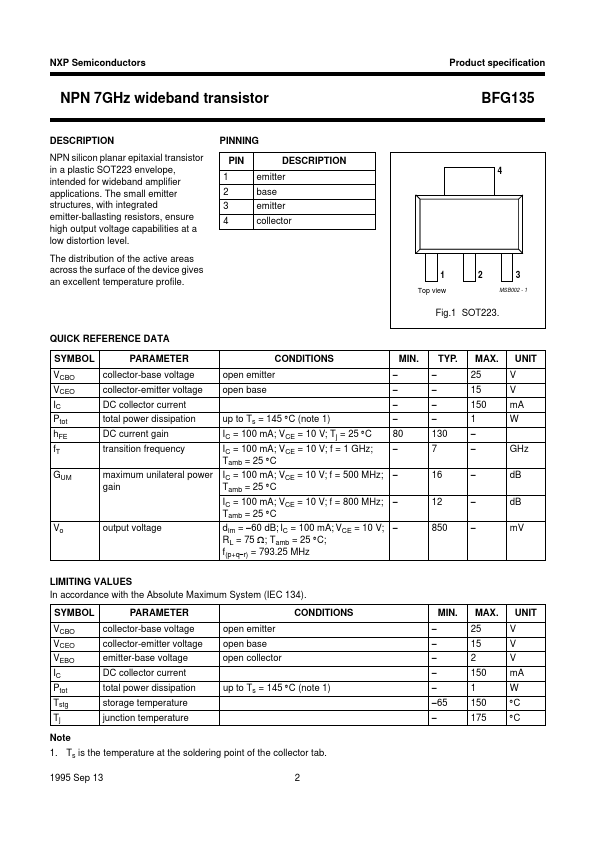
NPN silicon planar epitaxial transistor in a plastic SOT223 envelope, intended for wideband amplifier applications. PINNING PIN 1 2 3 4DESCRIPTION
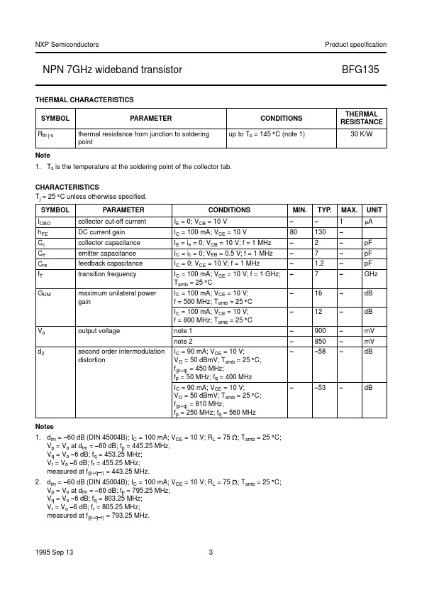
emitter base emitter collector lfpage 4 1 Top view 2 3 MSB002 - 1 Fig.1 SOT223. QUICK REFERENCE DATA SYMBOL PARAMETER CONDITIONS MIN. VCBO VCEO IC Ptot hFE fT GUM Vo collector-base voltage open emitter collector-emitter voltage open base DC collector current total power dissipation up to Ts = 145 C (note 1) DC current gain IC = 100 mA; VCE = 10 V; Tj = 25 C 80 transition frequency IC = 100 mA; VCE = 10 V; f = 1 GHz; Tamb = 25 C maximum unilateral power IC = 100 mA; VCE = 10 V; f = 500 MHz; gain Tamb = 25 C IC = 100 mA; VCE = 10 V; f = 800 MHz; Tamb = 25 C output voltage dim = 60 dB; IC = 100 mA; VCE = 10 V; RL = 75 ; Tamb = 25 C; f(p+qr) = 793.25 MHz TYP. 130 7 16 12 850 MAX. 25 15 150 1 UNIT V V mA W GHz dB dB mV LIMITING VALUES In accordance with the Absolute Maximum System (IEC 134).