BUK102-50GL
BUK102-50GL is PowerMOS transistor Logic level TOPFET manufactured by NXP Semiconductors.
DESCRIPTION
Monolithic temperature and overload protected logic level power MOSFET in a 3 pin plastic envelope, intended as a general purpose switch for automotive systems and other applications.
QUICK REFERENCE DATA
SYMBOL VDS ID PD Tj RDS(ON) PARAMETER Continuous drain source voltage Continuous drain current Total power dissipation Continuous junction temperature Drain-source on-state resistance VIS = 5 V MAX. 50 45 125 150 35 UNIT V A W ˚C mΩ
APPLICATIONS
General controller for driving lamps motors solenoids heaters
FEATURES
Vertical power DMOS output stage Low on-state resistance Overload protection against over temperature Overload protection against short circuit load Latched overload protection reset by input 5 V input level Low threshold voltage also allows 5 V control Control of power MOSFET and supply of overload protection circuits derived from input ESD protection on input pin Overvoltage clamping for turn off of inductive loads
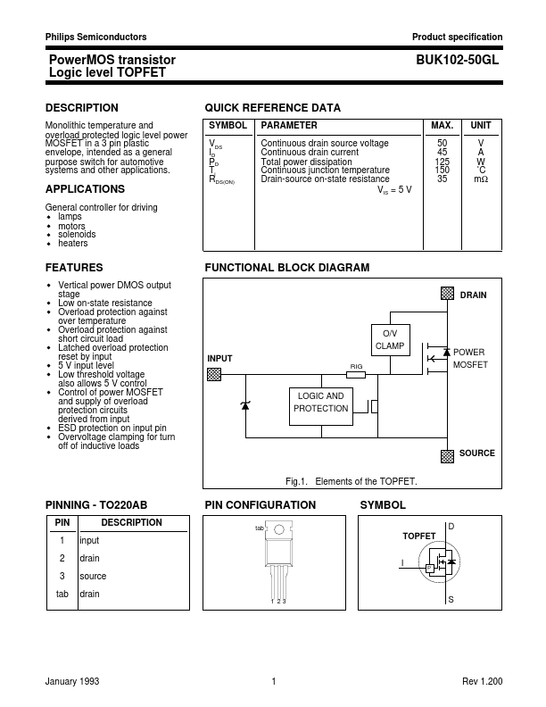
FUNCTIONAL BLOCK DIAGRAM
DRAIN
O/V CLAMP INPUT
POWER MOSFET
LOGIC AND PROTECTION
SOURCE
Fig.1. Elements of the TOPFET.
PINNING
- TO220AB
PIN 1 2 3 tab input drain source drain DESCRIPTION
PIN CONFIGURATION tab
SYMBOL
D TOPFET I
1 23
January 1993
Rev 1.200
Philips Semiconductors
Product specification
Power MOS transistor Logic level TOPFET
LIMITING VALUES
Limiting values in accordance with the Absolute Maximum Rating System (IEC 134) SYMBOL VDSS VIS ID ID IDRM PD Tstg Tj Tsold PARAMETER Continuous off-state drain source voltage1 Continuous input voltage Continuous drain current Continuous drain current Repetitive peak on-state drain current Total power dissipation Storage temperature Continuous junction temperature2 Lead temperature CONDITIONS VIS = 0 V Tmb ≤ 25 ˚C; VIS = 5 V Tmb ≤ 100 ˚C; VIS = 5 V Tmb ≤ 25 ˚C; VIS = 5 V Tmb ≤ 25 ˚C normal operation during soldering MIN. 0 -55
- BUK102-50GL
MAX. 50 6 45 28 180 125 150 150 250
UNIT V V A A A W ˚C ˚C ˚C
OVERLOAD PROTECTION LIMITING...