BUK7621-30
BUK7621-30 is TrenchMOS transistor Standard level FET manufactured by NXP Semiconductors.
DESCRIPTION
N-channel enhancement mode standard level field-effect power transistor in a plastic envelope suitable for surface mounting using ’trench’ technology. The device features very low on-state resistance and has integral zener diodes giving ESD protection up to 2k V. It is intended for use in automotive and general purpose switching applications.
QUICK REFERENCE DATA
SYMBOL VDS ID Ptot Tj RDS(ON) PARAMETER Drain-source voltage Drain current (DC) Total power dissipation Junction temperature Drain-source on-state resistance VGS = 10 V MAX. 30 50 94 175 21 UNIT V A W ˚C mΩ
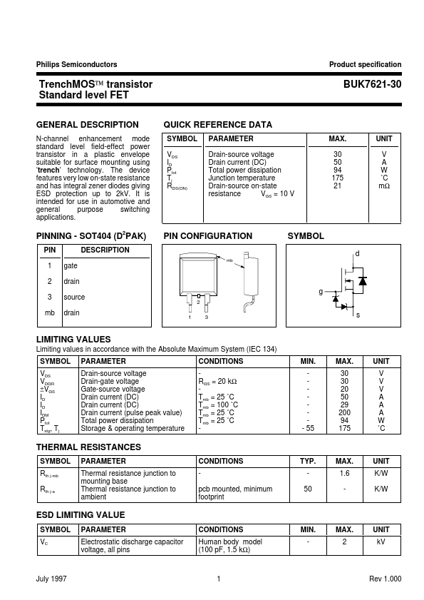
PINNING
- SOT404 (D2PAK)
PIN 1 2 3 mb gate drain source drain DESCRIPTION
PIN CONFIGURATION mb
SYMBOL d g
2 1 3 s
LIMITING VALUES
Limiting values in accordance with the Absolute Maximum System (IEC 134) SYMBOL VDS VDGR ±VGS ID ID IDM Ptot Tstg, Tj PARAMETER Drain-source voltage Drain-gate voltage Gate-source voltage Drain current (DC) Drain current (DC) Drain current (pulse peak value) Total power dissipation Storage & operating temperature CONDITIONS RGS = 20 kΩ Tmb = 25 ˚C Tmb = 100 ˚C Tmb = 25 ˚C Tmb = 25 ˚C MIN.
- 55 MAX. 30 30 20 50 29 200 94 175 UNIT V V V A A A W ˚C
THERMAL RESISTANCES
SYMBOL Rth j-mb Rth j-a PARAMETER Thermal resistance junction to mounting base Thermal resistance junction to ambient CONDITIONS pcb mounted, minimum footprint TYP. 50 MAX. 1.6 UNIT K/W K/W
ESD LIMITING VALUE
SYMBOL VC PARAMETER Electrostatic discharge capacitor voltage, all pins CONDITIONS Human body model (100 p F, 1.5 kΩ) MIN. MAX. 2 UNIT k V
July 1997
Rev 1.000
Philips Semiconductors
Product specification
Trench MOS™ transistor Standard level FET
STATIC CHARACTERISTICS
Tj= 25˚C unless otherwise specified SYMBOL V(BR)DSS VGS(TO) IDSS IGSS ±V(BR)GSS RDS(ON) PARAMETER Drain-source breakdown voltage Gate threshold voltage Zero gate voltage drain current Gate source leakage current CONDITIONS VGS = 0 V; ID = 0.25 m A; Tj = -55˚C VDS = VGS; ID = 1 m A Tj = 175˚C Tj = -55˚C VDS = 30...