BUK9605-30A
BUK9605-30A is TrenchMOS transistor Logic level FET manufactured by NXP Semiconductors.
DESCRIPTION
N-channel enhancement mode logic level field-effect power transistor in a plastic envelope suitable for surface mounting. Using ’trench’ technology the device features very low on-state resistance. It is intended for use in automotive and general purpose switching applications.
QUICK REFERENCE DATA
SYMBOL VDS ID Ptot Tj RDS(ON) PARAMETER Drain-source voltage Drain current (DC) Total power dissipation Junction temperature Drain-source on-state resistance VGS = 5 V VGS = 10 V MAX. 30 75 230 175 5 4.6 UNIT V A W ˚C mΩ mΩ
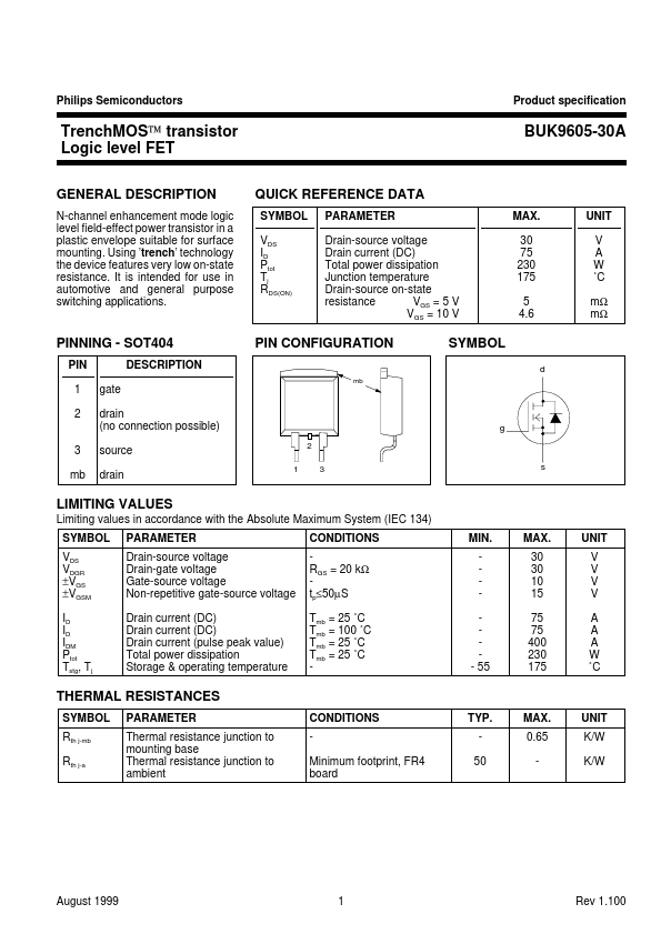
PINNING
- SOT404
PIN 1 2 3 mb gate drain (no connection possible) source drain DESCRIPTION
PIN CONFIGURATION mb
SYMBOL d g
2 1 3 s
LIMITING VALUES
Limiting values in accordance with the Absolute Maximum System (IEC 134) SYMBOL VDS VDGR ±VGS ±VGSM ID ID IDM Ptot Tstg, Tj PARAMETER Drain-source voltage Drain-gate voltage Gate-source voltage Non-repetitive gate-source voltage Drain current (DC) Drain current (DC) Drain current (pulse peak value) Total power dissipation Storage & operating temperature CONDITIONS RGS = 20 kΩ tp≤50µS Tmb = 25 ˚C Tmb = 100 ˚C Tmb = 25 ˚C Tmb = 25 ˚C MIN.
- 55 MAX. 30 30 10 15 75 75 400 230 175 UNIT V V V V A A A W ˚C
THERMAL RESISTANCES
SYMBOL Rth j-mb Rth j-a PARAMETER Thermal resistance junction to mounting base Thermal resistance junction to ambient CONDITIONS Minimum footprint, FR4 board TYP. 50 MAX. 0.65 UNIT K/W K/W
August 1999
Rev 1.100
Philips Semiconductors
Product specification
Trench MOS™ transistor Logic level FET
STATIC CHARACTERISTICS
Tj= 25˚C unless otherwise specified SYMBOL V(BR)DSS VGS(TO) IDSS IGSS RDS(ON) PARAMETER Drain-source breakdown voltage Gate threshold voltage Zero gate voltage drain current Gate source leakage current Drain-source on-state resistance CONDITIONS VGS = 0 V; ID = 0.25 m A; Tj = -55˚C VDS = VGS; ID = 1 m A Tj = 175˚C Tj = -55˚C VDS = 30 V; VGS = 0 V; VGS = ±10 V; VDS = 0 V VGS = 5 V; ID = 25 A VGS = 10 V; ID = 25 A VGS = 4.5 V; ID = 25 A Tj =...