FEATURES
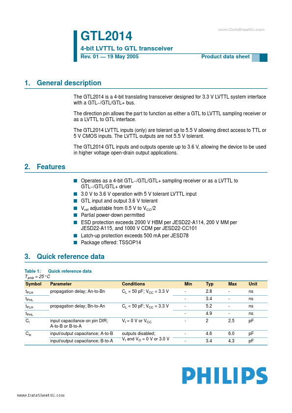
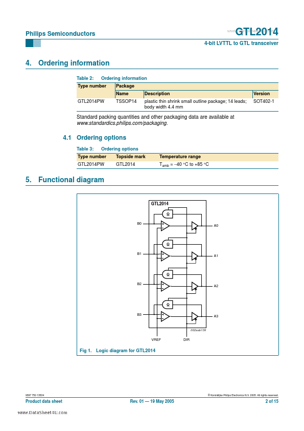
s Operates as a 4-bit GTL−/GTL/GTL+ sampling receiver or as a LVTTL to GTL−/GTL/GTL+ driver s 3.0 V to 3.6 V operation with 5 V tolerant LVTTL input s GTL input and output 3.6 V tolerant s Vref adjustable from 0.5 V to VCC/2 s Partial power-down permitted s ESD protection exceeds 2000 V HBM per JESD22-A114, 200 V MM per JESD22-A115, and 1000 V CDM per JESD22-CC101 s Latch-up protection exceeds 500 mA per JESD78 s Package offered: TSSOP14 3. Quick reference data Table 1: Quick reference data Tamb = 25 °C Symbol tPLH tPHL tPLH tPHL Ci Cio input capacitance on pin DIR; A-to-B or B-to-A input/output capacitance; A-to-B input/output capacitance; B-to-A VI = 0 V or VCC outputs disabled; VI and VO = 0 V or 3.0 V propagation delay; Bn-to-An CL = 50 pF; VCC = 3.3 V Parameter propagation delay; An-to-Bn Conditions CL = 50 pF; VCC = 3.3 V Min Typ 2.8 3.4 5.2 4.9 2 4.6 3.4 Max 2.5 6.0 4.3 Unit ns ns ns ns pF pF pF Philips Semiconductors GTL2014 4-bit LVTTL to GTL transceiver 4. Ordering information Table 2: Ordering information Package Name GTL2014PW TSSOP14 DESCRIPTION
plastic thin shrink small outline package; 14 leads; body width 4. NXP Semiconductors