DESCRIPTION
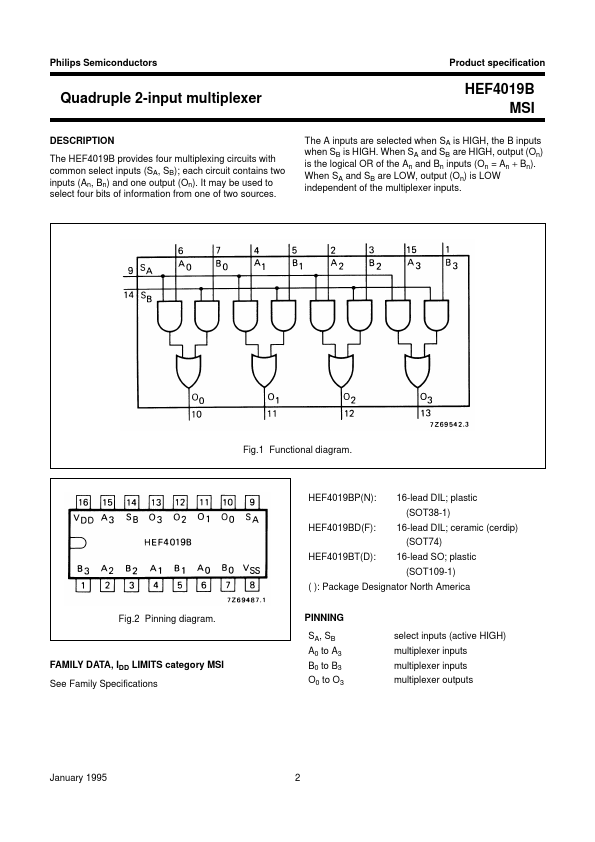
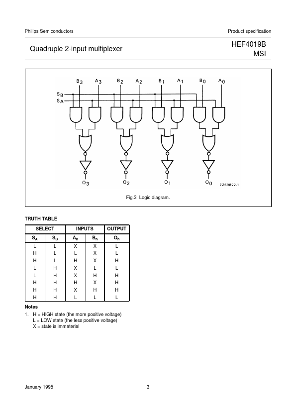
HEF4019B MSI The A inputs are selected when SA is HIGH, the B inputs when SB is HIGH. When SA and SB are LOW, output (On) is LOW independent of the multiplexer inputs. Fig.1 Functional diagram. HEF4019BP(N): HEF4019BD(F): HEF4019BT(D): 16-lead DIL; plastic (SOT38-1) 16-lead DIL; ceramic (cerdip) (SOT74) 16-lead SO; plastic (SOT109-1) ( ): Package Designator North America PINNING SA, SB A0 to A3 FAMILY DATA, IDD LIMITS category MSI See Family Specifications B0 to B3 O0 to O3 select inputs (active HIGH) multiplexer inputs multiplexer inputs multiplexer outputs Fig.2 Pinning diagram. January 1995 2 Philips Semiconductors Product specification Quadruple 2-input multiplexer HEF4019B MSI Fig.3 Logic diagram. TRUTH TABLE SELECT SA L H H L L H H H Notes 1. H = HIGH state (the more positive voltage) L = LOW state (the less positive voltage) X = state is immaterial SB L L L H H H H H INPUTS An X L H X X H X L Bn X X X L H X H L OUTPUT On L L H L H H H L January 1995 3 Philips Semicond... NXP Semiconductors