IRLZ34N
IRLZ34N is N-Channel MOSFET manufactured by NXP Semiconductors.
DESCRIPTION
N-channel enhancement mode logic level field-effect power transistor in a plastic envelope using ’trench’ technology. The device features very low on-state resistance and has integral zener diodes giving ESD protection up to 2k V. It is intended for use in switched mode power supplies and general purpose switching applications.
QUICK REFERENCE DATA
SYMBOL VDS ID Ptot Tj RDS(ON) PARAMETER Drain-source voltage Drain current (DC) Total power dissipation Junction temperature Drain-source on-state resistance VGS = 10 V MAX. 55 30 68 175 35 UNIT V A W ˚C mΩ
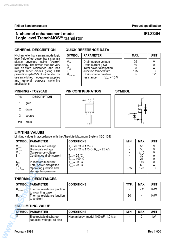
PINNING
- TO220AB
PIN 1 2 3 tab gate drain source drain DESCRIPTION
PIN CONFIGURATION tab
SYMBOL d g s
1 23
LIMITING VALUES
Limiting values in accordance with the Absolute Maximum System (IEC 134) SYMBOL PARAMETER VDSS VDGR VGS ID IDM PD Tj, Tstg Drain-source voltage Drain-gate voltage Gate-source voltage Continuous drain current Pulsed drain current Total power dissipation Operating junction and storage temperature CONDITIONS Tj = 25 ˚C to 175˚C Tj = 25 ˚C to 175˚C; RGS = 20 kΩ Tmb = 25 ˚C Tmb = 100 ˚C Tmb = 25 ˚C Tmb = 25 ˚C MIN.
- 55 MAX. 55 55 ± 13 30 21 110 68 175 UNIT V V V A A A W ˚C ta S hee t4U .co
THERMAL RESISTANCES
SYMBOL PARAMETER Rth j-mb Rth j-a Thermal resistance junction to mounting base Thermal resistance junction to ambient CONDITIONS TYP. 60 MAX. 2.2 UNIT K/W K/W
ESD LIMITING VALUE
SYMBOL PARAMETER VC Electrostatic discharge capacitor voltage, all pins CONDITIONS Human body model (100 p F, 1.5 kΩ) MIN. MAX. 2 UNIT k V ww w.D a
February 1999 m
Rev 1.000
..
Philips Semiconductors
Product specification
N-channel enhancement mode Logic level Trench MOSTM transistor
ELECTRICAL CHARACTERISTICS
Tj= 25˚C unless otherwise specified SYMBOL PARAMETER V(BR)DSS V(BR)GSS VGS(TO) RDS(ON) gfs IGSS IDSS Qg(tot) Qgs Qgd td on tr td off tf Ld Ld Ls Ciss Coss Crss Drain-source breakdown voltage Gate-source breakdown voltage Gate threshold voltage Drain-source on-state resistance...