MPC17529
MPC17529 is dual H-Bridge motor driver manufactured by NXP Semiconductors.
NXP Semiconductors Technical Data
0.7 A dual H-Bridge motor driver with 3.0 V/5.0 V patible logic I/O
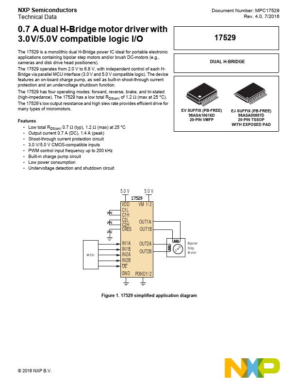
The 17529 is a monolithic dual H-Bridge power IC ideal for portable electronic applications containing bipolar step motors and/or brush DC-motors (e.g., cameras and disk drive head positioners). The 17529 operates from 2.0 V to 6.8 V, with independent control of each HBridge via parallel MCU interface (3.0 V and 5.0 V patible logic). The device Features an on-board charge pump, as well as built-in shoot-through current protection and an undervoltage shutdown function. The 17529 has four operating modes: forward, reverse, brake, and tri-stated (high-impedance). The 17529 has a low...